


FA Lenses | How to Achieve Precision Defect Detection in the 3C Industry?
I. Testing Requirements in the 3C Industry and Core Advantages of FA Lenses

1. Detection Pain Points:
3C products (such as mobile phones, laptops, and PCBs) feature minute dimensions (0.1-1mm-level defects), complex structures (curved surfaces, multi-layer stacking), and high precision requirements (micron-level tolerances). Traditional manual or conventional visual inspection methods are prone to missed defects or misjudgments.
2. FA Lens Value:
① Low distortion characteristics: Distortion is controlled below 0.5% through optical design (e.g., ultra-low dispersion glass, symmetrical lens groups), ensuring consistent edge-to-center image proportions. This prevents measurement errors or defect misclassification caused by distortion (e.g., scratches on phone casings, PCB solder joint misalignment).
② Uniform Light Distribution: Combining ring/coaxial light sources achieves illumination intensity variation <5% across the detection area, eliminating shadows/bright spots. This enhances visibility and recognition accuracy for minute defects (e.g., 0.1mm-level scratches, point-like foreign objects).
II. Key Technology Implementation Pathways

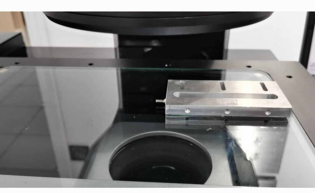
1. Optical System Design
-
Lens Selection: 360° Outer/Inner Wall Lens: Utilizes a diffractive-reflective optical path to enable a single camera and lens to cover the entire circumference of objects (e.g., bottle caps, screws), simplifying multi-camera systems and reducing costs. Octagonal Prism Lens: Extends detection range to 5-70mm, supporting simultaneous inner and outer wall inspection.
-
Lighting Solution: Ring Light + Diffuser Panel: Uniformly illuminates curved/reflective surfaces (e.g., smartphone glass covers) to minimize glare interference; employs High Dynamic Range (HDR) technology to composite multi-exposure images, addressing unevenly lit scenes.
2. Algorithms and Software Systems
-
Deep Learning + Traditional Algorithm Integration: Deep learning (e.g., YOLO, ResNet) identifies complex defects (e.g., character defects, shrinkage marks), addressing issues like positional fluctuations and color variations; traditional algorithms (edge detection, pattern matching) handle regular defects (e.g., dimensional deviations, holes).
-
System Function Integration: Automated Inspection Process: Automatic labeling, report generation, historical records, and anomaly alerts; supports simultaneous inspection of multiple components (e.g., internal laptop screws, foam pads, ribbon cables). Real-time yield statistics and defect distribution tracking, with batch traceability and quality analysis capabilities (e.g., Guichen Robotics systems record defect locations and sizes per product roll for grading and classification).
3. Typical Scenario Case Studies
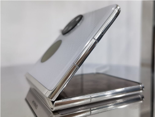
① Mobile Phone Case Inspection: Detects scratches, indentations, plating peeling, and specks of foreign matter with precision down to 0.3mm.
② PCB/FPC Inspection: AOI equipment detects solder joints, open/short circuits, and character defects with precision of 1.5μm (laser line width 1-5μm).
③ Laptop Internal Inspection: Fully automated detection of protruding screws, flex cable connector height, and antenna port polarity identification.

Product recommendation
TECHNICAL SOLUTION
MORE+You may also be interested in the following information
FREE CONSULTING SERVICE
Let’s help you to find the right solution for your project!

 ASK POMEAS
  PRICE INQUIRY
  REQUEST DEMO/TEST
  FREE TRIAL UNIT
  ACCURATE SELECTION
 - APPICATION CASE
- RESOURCE CENTER
- DOWNLOAD CENTER
SOLUTIONS SUPPORT
- ZOOM LENS SELECTION TOOL
- TELECENTRIC LENS SELECTION TOOL
- FA LENS SELECTION TOOL
- ZOOM RATIO TABLE
- CERTIFIED MODEL
SELECTION TOOL
- WHY POMEAS
- FAQ
- PRIVACY POLICY
- TERMS OF USE
- DELIVERY & RETURN POLICY
CUSTOMER CARE
 ADDRESS
Add.:No.68, Chongwei Road, Baizhoubian, East district, Dongguan, China, 523000
CONTACT
 Tel:+ 86-0769-2266 0867
 Fax:+ 86-0769-2266 0867
 E-mail:marketing@pomeas.com

Wechat QR code
Software Copyright :2021SR0176001 抄袭必究, 技术支持:誉新源科技