


How does an electric ZOOM LENS achieve “wide-angle scanning followed by close-up inspection”?
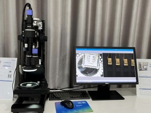
In the field of industrial inspection, motorized ZOOM LENS achieve seamless integration between rapid positioning with a wide field of view and precise inspection within a narrow field of view through an automated workflow of “wide-angle scanning followed by close-up inspection.” This significantly enhances inspection efficiency and accuracy. Taking PCB-AOI (automated optical inspection) and semiconductor packaging inspection as examples, we will analyze their technical implementation pathways and core advantages.
I. Technical Principle: Dual-Mode Coordination Mechanism for Motorized ZOOM LENS
The core function of an electric ZOOM LENS lies in its ability to achieve continuous focal length adjustment through the precise movement of optical components (such as lens groups) driven by internal motors. Its operational workflow can be divided into two stages:
1. Wide-angle survey stage: The lens operates at low magnification (e.g., 0.7X) to cover a broad field of view (e.g., an entire PCB board or semiconductor wafer), rapidly scanning the target area to locate potential defects or anomalies.
2. Close-up Inspection Phase: The lens automatically switches to high magnification (e.g., 4.5X), focusing on anomalous areas. It captures detailed features through high-resolution imaging (e.g., over 200 line pairs per millimeter resolution) to provide data support for subsequent analysis.
This process is achieved through deep integration of software algorithms and hardware drivers: the system automatically triggers zoom commands based on preset rules (e.g., defect type, position coordinates). Motor-driven lenses complete focal length switching within milliseconds, while image sensors simultaneously adjust exposure parameters to ensure stable image quality.
II. Application Scenario 1: PCB-AOI Inspection—Precision Screening from Global to Local
On PCB production lines, AOI equipment must detect minute defects such as solder joint defects, circuit shorts, and component misalignment. Traditional solutions require multiple fixed-magnification lenses for sequential inspection, whereas motorized ZOOM LENS enable end-to-end inspection through a single system:

1. Wide-angle inspection: Scans the entire PCB board at 0.7X magnification, rapidly identifying suspicious areas (such as solder joint clusters and chip packaging zones) through image processing algorithms (e.g., edge detection, template matching).

2. Close-up Inspection: For suspicious areas, the lens automatically switches to 3X-5X magnification. Combined with AI image recognition technology (such as deep learning models), it analyzes details like solder joint morphology and circuit spacing to determine whether a defect is genuine.
III. Application Scenario 2: Semiconductor Packaging Inspection—Micrometer-Level Defect Tracking with Magnifying Glass Precision
The semiconductor packaging process demands extremely high standards of cleanliness and precision, requiring inspection for micron-level defects such as bent leads, wafer scratches, and encapsulation bubbles. Motorized ZOOM LENS achieve efficient inspection through the following workflow:
1. Wide-angle inspection: Scan the entire package module (e.g., BGA chip) at 1X magnification. Utilize multispectral imaging technology (e.g., infrared + visible light fusion) to locate abnormal hotspots or reflective anomalies.
2. Close-up Inspection: Switch to 10X-20X magnification and combine with laser confocal technology to perform 3D topography reconstruction of anomalies, quantifying defect dimensions (e.g., pin bending angle, bubble depth).
IV. Core Advantages: Balancing Efficiency, Flexibility, and Cost
1. Efficiency Enhancement: Replacing multi-lens systems with a single lens reduces mechanical switching time (traditional solutions require moving the stage or changing lenses, taking several seconds). The motorized ZOOM LENS completes focal length switching within 0.5 seconds, boosting inspection speed by over 3 times.
2. Flexibility Boost: Software-defined inspection workflows adapt to workpieces of varying sizes and types (e.g., from mobile phone PCBs to server motherboards) without requiring optical system redesign.
3. Cost Optimization: Reduced lens count and mechanical complexity lower equipment maintenance costs.
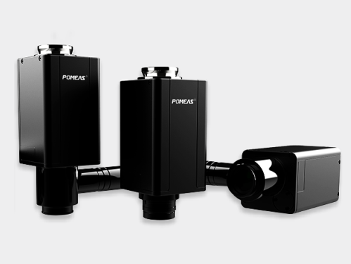
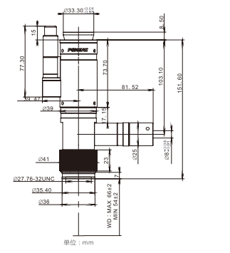
Product recommendation
TECHNICAL SOLUTION
MORE+You may also be interested in the following information
FREE CONSULTING SERVICE
Let’s help you to find the right solution for your project!

 ASK POMEAS
  PRICE INQUIRY
  REQUEST DEMO/TEST
  FREE TRIAL UNIT
  ACCURATE SELECTION
 - APPICATION CASE
- RESOURCE CENTER
- DOWNLOAD CENTER
SOLUTIONS SUPPORT
- ZOOM LENS SELECTION TOOL
- TELECENTRIC LENS SELECTION TOOL
- FA LENS SELECTION TOOL
- ZOOM RATIO TABLE
- CERTIFIED MODEL
SELECTION TOOL
- WHY POMEAS
- FAQ
- PRIVACY POLICY
- TERMS OF USE
- DELIVERY & RETURN POLICY
CUSTOMER CARE
 ADDRESS
Add.:No.68, Chongwei Road, Baizhoubian, East district, Dongguan, China, 523000
CONTACT
 Tel:+ 86-0769-2266 0867
 Fax:+ 86-0769-2266 0867
 E-mail:marketing@pomeas.com

Wechat QR code
Software Copyright :2021SR0176001 抄袭必究, 技术支持:誉新源科技