


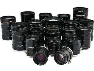
High-magnification FA microscope lenses for PCB and semiconductor inspection applications
In the fields of PCB (printed circuit board) and semiconductor manufacturing, solder joint misalignments at the 0.1mm level, circuit defects at the micrometer level, and chip cracks at the nanometer level can all lead to product failure. High-magnification FA microscope lenses serve as the “eagle eyes” of industrial vision inspection. With their ultra-high resolution and precise magnification capabilities, paired with high-resolution cameras, they clearly reveal the microscopic world, making them core equipment for defect detection.

I. Core Principle: High Magnification + High Resolution, Pushing the Boundaries of Microscopic Observation
PCB trace widths and semiconductor chip pin pitches have reached the micrometer and even submicrometer levels, making it difficult for ordinary lenses to capture clear details. The core advantage of high-magnification FA microscope lenses lies in their dual capabilities of “precise magnification + detail restoration”:
-
Ultra-high magnification coverage for microscopic scenes: Supports 0.5X-10X magnification adjustment or even higher (some lenses can extend to 20X with extension tubes), magnifying 10μm circuit defects to a scale visible to the naked eye. Whether it's solder pad oxidation or circuit shorts on PCBs, or broken bonding wires and wafer scratches on semiconductor chips, all can be precisely captured.
-
High resolution matched to camera performance: Lens resolution typically exceeds 100 lines per millimeter (lp/mm). Paired with high-resolution industrial cameras ranging from 5 to 20 megapixels, it achieves “pixel-level” detail reproduction. For example, a 20-megapixel camera paired with a 2X magnification FA lens can map a 1μm defect across multiple pixels, preventing detail loss due to insufficient resolution and providing clear evidence for defect determination.
-
Low distortion ensures measurement accuracy: Industrial-grade high-magnification FA lenses employ specialized optical designs, controlling distortion rates below 0.1%—significantly outperforming standard consumer microscope lenses. In applications like PCB trace width measurement and semiconductor chip pin pitch inspection, low distortion guarantees precise scaled images, eliminating measurement errors caused by image distortion.
II. Key Characteristics: The Art of Balancing Working Distance and Depth of Field
PCB and semiconductor inspection scenarios impose clear requirements on operational space and inspection efficiency. The working distance and depth of field design of high-magnification FA microscope lenses directly determine inspection feasibility and stability:
1. Working distance: Balancing operational space and magnification effect
Working distance refers to the distance from the front of the lens to the object being measured. This parameter is particularly critical in PCB solder joint inspection and semiconductor chip packaging inspection:
- Moderate working distance prevents interference: High-magnification lenses typically feature a “long working distance design,” maintaining a working distance of 50mm-150mm even at 5X-10X magnification (some telecentric high-magnification lenses can exceed 200mm). This design provides ample operating space to prevent collisions between the lens and PCB boards or semiconductor packages. It also facilitates integration with auxiliary lighting equipment like ring lights or coaxial lights, enhancing defect contrast.
- Precise matching for inspection scenarios: For instance, in PCB automated optical inspection (AOI) equipment, lenses must coordinate with conveyor systems for continuous inspection. A long working distance prevents interference with conveyor mechanisms. In offline sampling inspections of semiconductor chips, medium working distance lenses can be selected to enhance magnification while maintaining operational space, enabling focus on finer internal chip defects.
2. Depth of Field Control: Balancing Clarity and Detection Efficiency
Depth of field refers to the range of objects that appear sharp in the image produced by a lens. At high magnifications, the depth of field is typically shallow (e.g., approximately 10μm at 1X magnification and potentially only 1μm at 10X magnification). However, through proper design and configuration, it can meet diverse inspection requirements:
- Shallow Depth of Field Highlights Defect Details: In detecting “planar defects” such as scratches on semiconductor chip surfaces or indentations in PCB pads, shallow depth of field allows clear focus on the defect area while blurring the background. This reduces interference from irrelevant information and enhances defect recognition efficiency. For instance, when inspecting nanoscale cracks on chip surfaces, precise focusing creates sharp contrast between crack edges and surrounding areas, enabling algorithms to quickly capture them.
- Multi-level depth of field captures three-dimensional defects: For “three-dimensional defects” like height variations in PCB solder joints or warped semiconductor package pins, multi-level depth of field photography can be achieved by adjusting lens focal length. Alternatively, an auto-focus module can automatically composite full-depth-of-field images, ensuring defects at varying heights are clearly visible. For instance, when inspecting PCB solder joint wetting, full-depth-of-field technology allows simultaneous clear observation of solder coverage on both the top and sides of the joint, enabling detection of cold solder joints or false soldering.
III. Practical Application: Case Studies of “Flaw Detection” in Two Major Fields
1. PCB Inspection: Comprehensive Quality Control from Circuitry to Solder Joints


- Circuit Defect Detection: PCB trace widths typically range from 3mil to 8mil (1mil = 25.4μm). Using a 4X high-magnification FA lens paired with a 12-megapixel camera, 3mil traces can be magnified to over 300μm, enabling clear identification of defects such as open circuits, short circuits, and uneven etching. The lens's high-contrast design enhances brightness differences between traces and substrates, enabling precise detection of even minute trace gaps.
- Solder Joint Quality Inspection: In SMT (Surface Mount Technology) processes, solder joint size, shape, and solder coverage directly impact connection reliability. High-magnification FA lenses magnify solder joint details to identify issues like bridging, cold solder joints, or insufficient solder. Combined with coaxial lighting, they also detect surface defects such as oxidation and bubbles, ensuring soldering quality meets standards.
2. Semiconductor Inspection: Precision Screening That Penetrates the Microscopic World


- Chip Packaging Inspection: During semiconductor chip packaging, defects such as pin deformation, bond wire breakage, and encapsulation resin cracks may occur. Using 8X-10X high-magnification FA lenses enables clear observation of whether pin pitch (typically 0.3mm-0.5mm) meets specifications, whether bonding wires (diameter only tens of micrometers) are broken or misaligned, and whether the encapsulation resin has micro-cracks. This prevents chip performance failures caused by packaging defects.
- Wafer Defect Inspection: Wafer fabrication is the core process in semiconductor production. Surface scratches, impurities, and pattern defects all impact chip yield. High-magnification FA microscope lenses paired with high-resolution cameras enable high-precision scanning of wafer surfaces, identifying nanoscale scratches and impurities. The lenses' low chromatic aberration design ensures accurate color reproduction in images, facilitating differentiation between defects of different materials (e.g., metallic impurities versus silicon-based scratches).
IV. Key Selection Criteria: Core Parameter Reference for Scenario Compatibility
When selecting high-magnification FA microscope objectives, it is essential to consider the specific requirements of PCB and semiconductor inspection, focusing on the following parameters:
1. Magnification Range: For PCB inspection, 1X-5X magnification is recommended to balance operational space and detail reproduction; for semiconductor chip inspection, 5X-10X magnification can be selected to focus on microscopic defects.
2. Resolution: Prioritize lenses with resolution ≥150 lp/mm paired with cameras exceeding 10 megapixels to ensure clear visualization of micron-level defects.
3. Working Distance: For inline inspection, select lenses with ≥80mm working distance to accommodate lighting and operational space. Offline sampling may use lenses within 50mm-120mm range as needed.
4. Distortion Rate: For measurement applications (e.g., line width, pin pitch measurement), select lenses with distortion ≤0.1% to ensure measurement accuracy.
5. Interface Compatibility: Must match camera interfaces (C-mount, F-mount, etc.) while considering lens flange distance to prevent focusing inaccuracies after installation.
Product recommendation
TECHNICAL SOLUTION
MORE+You may also be interested in the following information
FREE CONSULTING SERVICE
Let’s help you to find the right solution for your project!

 ASK POMEAS
  PRICE INQUIRY
  REQUEST DEMO/TEST
  FREE TRIAL UNIT
  ACCURATE SELECTION
 - APPICATION CASE
- RESOURCE CENTER
- DOWNLOAD CENTER
SOLUTIONS SUPPORT
- ZOOM LENS SELECTION TOOL
- TELECENTRIC LENS SELECTION TOOL
- FA LENS SELECTION TOOL
- ZOOM RATIO TABLE
- CERTIFIED MODEL
SELECTION TOOL
- WHY POMEAS
- FAQ
- PRIVACY POLICY
- TERMS OF USE
- DELIVERY & RETURN POLICY
CUSTOMER CARE
 ADDRESS
Add.:No.68, Chongwei Road, Baizhoubian, East district, Dongguan, China, 523000
CONTACT
 Tel:+ 86-0769-2266 0867
 Fax:+ 86-0769-2266 0867
 E-mail:marketing@pomeas.com

Wechat QR code
Software Copyright :2021SR0176001 抄袭必究, 技术支持:誉新源科技