


Application of 3D tool microscope for surface topography analysis of micro- and nanomaterials
In the semiconductor manufacturing process, 3D tool microscope can be used to detect tiny defects and contamination particles on the chip surface. By accurately measuring and analyzing its surface topography, problems in the manufacturing process can be detected and corrected in time, improving the quality and reliability of the chip.

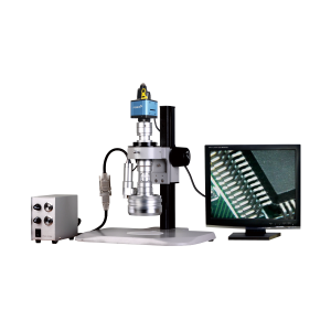
In the field of micro and nanomaterials science, accurate measurement and analysis of surface morphology is crucial for understanding the properties of materials, optimizing manufacturing processes, and developing new materials. 3D tool microscopy, as a high-precision, non-contact measurement device, shows great potential for application in the surface morphology analysis of micro and nanomaterials.
I. High Precision Measurement
3D tool microscopes are capable of capturing extremely minute details on the surface of micro- and nanomaterials through advanced optical systems and high-resolution image sensors. Its measurement accuracy usually reaches the nanometer level, enabling scientists and engineers to accurately obtain three-dimensional topographic data of the material surface, including height, roughness, corrugation and other key parameters.
II. Non-contact Inspection
Compared with traditional contact measurement tools, 3D tool microscope uses non-contact detection to avoid damage to the material surface during the measurement process. This is especially important for micro and nano materials, as their surfaces are often very fragile, and any minor scratches or damage may affect the overall performance of the material.
III. 3D Visualization and Data Analysis
The 3D tool microscope is not only able to provide high-precision measurement data, but also able to display the measurement results in the form of three-dimensional images. This three-dimensional visualization function allows scientists to intuitively observe and analyze the material surface morphology features, such as bumps, depressions, cracks, etc.. At the same time, combined with professional data analysis software, the measurement data can also be further processed and analyzed to extract more useful information.
In the semiconductor manufacturing process, 3D tool microscope can be used to detect tiny defects and contamination particles on the chip surface. By accurately measuring and analyzing its surface topography, problems in the manufacturing process can be detected and corrected in time, improving the quality and reliability of the chip.
Product recommendation
TECHNICAL SOLUTION
MORE+You may also be interested in the following information
FREE CONSULTING SERVICE
Let’s help you to find the right solution for your project!

 ASK POMEAS
  PRICE INQUIRY
  REQUEST DEMO/TEST
  FREE TRIAL UNIT
  ACCURATE SELECTION
 - APPICATION CASE
- RESOURCE CENTER
- DOWNLOAD CENTER
SOLUTIONS SUPPORT
- ZOOM LENS SELECTION TOOL
- TELECENTRIC LENS SELECTION TOOL
- FA LENS SELECTION TOOL
- ZOOM RATIO TABLE
- CERTIFIED MODEL
SELECTION TOOL
- WHY POMEAS
- FAQ
- PRIVACY POLICY
- TERMS OF USE
- DELIVERY & RETURN POLICY
CUSTOMER CARE
 ADDRESS
Add.:No.68, Yongwei Road, Baizhoubian, Dongcheng District, Dongguan, China,523000
CONTACT
 Tel:+ 86-0769-2266 0867
 Fax:+ 86-0769-2266 0867
 E-mail:marketing@pomeas.com

Wechat QR code
Software Copyright :2021SR0176001 抄袭必究, 技术支持:誉新源科技