


Program Pain Points:

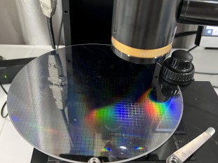
7nm and below node evolution, the wafer surface feature size is close to the physical limit, the traditional inspection equipment is facing two core contradictions: full-area scanning efficiency needs and nanometer defect detection accuracy requirements. Full-area scanning needs to cover the entire wafer (e.g., 12 inches), while local defect detection needs to capture sub-micron scratches, line width deviations and other microscopic defects.
Solution:

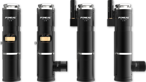
POMEAS' 4K zoom lens LZH series is paired with an intelligent detection solution for alarm industrial cameras, which realizes “global-local” synergistic detection through dynamic zoom technology.
Program Strengths:

1、Magnification between 0.68X~5X
The LZH series adopts an innovative optical design, supporting 0.68X~5X continuous zoom. In 7nm wafer inspection, 0.68X low-magnification mode can quickly complete the panoramic scanning of the entire wafer, while 5X high-magnification mode can be used for sub-micron magnification observation of suspected defect areas. Compared with the traditional fixed-magnification lens, the inspection efficiency is increased by more than 30%.
2、4K high resolution and large target surface fusion
Equipped with 1” large target surface sensor interface, LZH series still maintains 4K imaging resolution in high-magnification mode, with an object-square resolution of 2.8 μm/pixel, and combined with dynamic zoom compensation algorithms, it ensures that there is no distortion or center shift in the image during the zoom process, and realizes a seamless switching from macroscopic to microscopic.
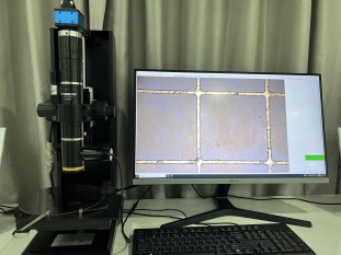
3、Motorized zoom and intelligent control
Integrated RS232/USB dual-interface motorized control system supports software programming to realize automatic varifocal. By presetting the inspection path, the system can complete the magnification switching in milliseconds, together with the high-precision displacement platform, to build a closed-loop inspection process of “global coarse screening - local fine inspection”.
POMEAS' wafer inspection solution with 4K zoom lens as the core, through innovative optical design and intelligent control technology, effectively solves the inspection contradiction between high precision and large field of view.
Product recommendation
TECHNICAL SOLUTION
MORE+You may also be interested in the following information
FREE CONSULTING SERVICE
Let’s help you to find the right solution for your project!

 ASK POMEAS
  PRICE INQUIRY
  REQUEST DEMO/TEST
  FREE TRIAL UNIT
  ACCURATE SELECTION
 - APPICATION CASE
- RESOURCE CENTER
- DOWNLOAD CENTER
SOLUTIONS SUPPORT
- ZOOM LENS SELECTION TOOL
- TELECENTRIC LENS SELECTION TOOL
- FA LENS SELECTION TOOL
- ZOOM RATIO TABLE
- CERTIFIED MODEL
SELECTION TOOL
- WHY POMEAS
- FAQ
- PRIVACY POLICY
- TERMS OF USE
- DELIVERY & RETURN POLICY
CUSTOMER CARE
 ADDRESS
Add.:No.68, Chongwei Road, Baizhoubian, East district, Dongguan, China, 523000
CONTACT
 Tel:+ 86-0769-2266 0867
 Fax:+ 86-0769-2266 0867
 E-mail:marketing@pomeas.com

Wechat QR code
Software Copyright :2021SR0176001 抄袭必究, 技术支持:誉新源科技