


In the field of semiconductor manufacturing, wafer inspection is a key link to ensure the quality of the chip, and the performance of the lens directly affects the accuracy and reliability of the inspection results. 14X zoom lens with its unique technical characteristics, in the wafer inspection shows significant advantages over the traditional 0.7X-4.5X zoom lens.

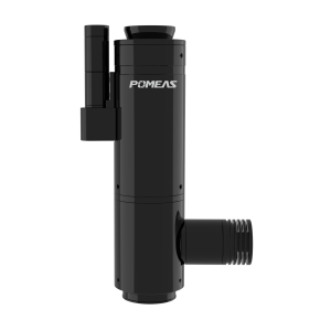
Optical magnification is the most intuitive difference between the two. 14X zoom lens has an optical magnification range of 0.55X~7.6X, while the traditional 0.7X-4.5X zoom lens has a relatively narrow magnification range. The 14X zoom lens is able to realize the fast macro scanning of the whole wafer under low magnification, and the precise observation of nanometer circuit lines and very small defects under high magnification.

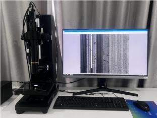
For example, when detecting the transistor gate structure on 7nm process wafers, traditional lenses have fuzzy imaging at high magnification, making it difficult to distinguish subtle line deformations; while the high-magnification feature of the 14X zoom lens can clearly present key parameters such as the width and spacing of the gate lines, discovering tiny defects that may affect the chip's performance, and raising the detection accuracy to a new height.

In terms of working distance, the 77.8mm working distance of the 14X zoom lens is shorter than the 87mm of conventional lenses, a feature that is extremely valuable in wafer inspection. The structure of the wafer surface is becoming increasingly complex and precise, and the shorter working distance enables the 14X zoom lens to focus more closely on the wafer surface, obtaining clearer and more detailed images when inspecting structures such as grooves with high depth-to-width ratios and tiny bumps. At the same time, a shorter working distance also helps to reduce the loss of light in the propagation process, improve the contrast and brightness of the imaging, so that the inspection system can more accurately identify the various types of defects on the wafer surface.
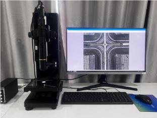
Imaging quality and depth of field control, 14X zoom lens is also outstanding. Traditional 0.7X-4.5X zoom lens at high magnification depth of field is shallow, in the detection of a certain height difference in the structure of the wafer, such as multi-layer interconnection of metal wiring, it is difficult to ensure that the different height levels of the level of the same time a clear image, which is prone to cause some of the regional details are lost, resulting in defects missed. 14X zoom lens through the advanced optical design and optimization, the depth of field can still be maintained at high magnification is still relatively good, when detecting three-dimensional structure of the wafer, such as multi-layer interconnections. When detecting the three-dimensional structure of the wafer, it can more comprehensively present the details of each layer of the structure, whether it is a raised soldering point or a recessed etching groove, which can be clearly displayed, effectively reducing the risk of detection due to the lack of depth of field.
In addition, the 14X zoom lens also has advantages in inspection efficiency. Its wide range of magnification reduces the frequency of lens replacement during the inspection process, without the need for frequent switching of equipment parameters can be completed with different precision requirements of the inspection task, greatly improving the overall efficiency of wafer inspection. In large-scale wafer production line, time is cost, 14X zoom lens of efficient detection ability to help improve the output of the production line, for enterprises to create greater economic benefits.
TECHNICAL SOLUTION
MORE+You may also be interested in the following information
FREE CONSULTING SERVICE
Let’s help you to find the right solution for your project!

 ASK POMEAS
  PRICE INQUIRY
  REQUEST DEMO/TEST
  FREE TRIAL UNIT
  ACCURATE SELECTION
 - APPICATION CASE
- RESOURCE CENTER
- DOWNLOAD CENTER
SOLUTIONS SUPPORT
- ZOOM LENS SELECTION TOOL
- TELECENTRIC LENS SELECTION TOOL
- FA LENS SELECTION TOOL
- ZOOM RATIO TABLE
- CERTIFIED MODEL
SELECTION TOOL
- WHY POMEAS
- FAQ
- PRIVACY POLICY
- TERMS OF USE
- DELIVERY & RETURN POLICY
CUSTOMER CARE
 ADDRESS
Add.:No.68, Chongwei Road, Baizhoubian, East district, Dongguan, China, 523000
CONTACT
 Tel:+ 86-0769-2266 0867
 Fax:+ 86-0769-2266 0867
 E-mail:marketing@pomeas.com

Wechat QR code
Software Copyright :2021SR0176001 抄袭必究, 技术支持:誉新源科技