


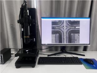
In the semiconductor manufacturing industry, wafers are the core components that require high precision and quality control during the manufacturing process. 14X zoom lens inspection solution, with 14X zoom lens as the core, high-definition industrial camera, built-in coaxial and external ring light, and POMEAS MetX multisensor measurement system, is designed to provide a set of high-resolution, flexible, accurate and efficient solutions for wafer inspection. It is designed to provide a high-resolution, highly flexible, accurate and efficient solution for wafer inspection, capable of comprehensively and accurately detecting all kinds of defects and features on the surface of wafers as well as inside wafers, to meet the increasingly demanding quality control needs of the semiconductor industry.

Program components
( A )14X Zoom Lens

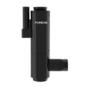
The 14X zoom lens has excellent optical performance, its 14 times zoom ability can be flexibly switched at different magnification, to realize the fine observation and inspection of different areas of the wafer, different size features. In wafer surface defect detection, low magnification can be used for rapid scanning of the wafer as a whole, a comprehensive grasp of the macroscopic state of the wafer, and efficiently screen out areas with obvious defects; high magnification can focus on small defects, such as nanometer scratches, holes, particles, contaminants, and so on, to clearly present the details of the defects, which makes it easy for the inspector or the system to accurately identify and analyze, and ensures that no small defects will be spared. defects.
( B )High Definition Industrial Camera

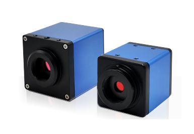
The HD industrial camera works closely with the 14X zoom lens, featuring high resolution and high frame rate. It can quickly and clearly convert the wafer images captured by the lens into digital signals to ensure that the images are rich in details and true colors. Even in the high-speed inspection process, it can also stably output high-quality images to avoid the accuracy of the inspection results due to image blurring, distortion and other problems. In addition, its powerful data transmission capability can quickly transfer the captured images to the subsequent processing system, providing strong support for efficient inspection processes.
( C )Built-in coaxial optical and external ring optical

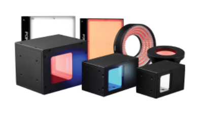
1. Built-in coaxial optical:The built-in coaxial light illuminates the wafer surface vertically, which can illuminate the wafer uniformly and eliminate the shadows caused by the uneven surface, so that defects such as tiny undulations, pits, scratches, etc. on the surface of the wafer are more clearly visible. For wafers with extremely high surface finish requirements, the coaxial light can accurately detect minor surface defects, avoiding missed inspections, while ensuring the contrast and clarity of the image, providing a good visual basis for defect identification.
2. External ring light:The external ring light irradiates the wafer from different angles around the wafer, which can emphasize the three-dimensional characteristics of the wafer surface, and has excellent detection effect for defects such as bumps and granular contaminants. It cooperates with the built-in coaxial light to form a multi-angle, omni-directional illumination system, regardless of the shape and location of the defects on the wafer surface, it can be effectively illuminated and detected, which significantly improves the comprehensiveness and accuracy of the detection.
( D )POMEAS MetX Multi Sensor Measurement System

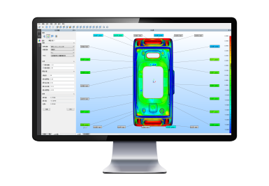
The POMEAS MetX multi-sensor measurement system is the intelligent core of the entire inspection solution. It integrates advanced image processing algorithms and data analysis technologies to quickly process and analyze wafer images captured by high-definition industrial cameras. By accurately identifying and quantifying the shape, size, location and other information of defects in the image, it realizes automatic classification and grading of wafer defects, and determines whether the wafer meets quality standards. At the same time, the system is also able to record and store inspection data and generate detailed inspection reports, providing powerful data support for quality traceability and process optimization in the production process. In addition, the MetX system has good compatibility and scalability, and can flexibly adjust the inspection parameters and algorithms according to different wafer inspection needs, adapting to diversified production scenarios.
Product recommendation
TECHNICAL SOLUTION
MORE+You may also be interested in the following information
FREE CONSULTING SERVICE
Let’s help you to find the right solution for your project!

 ASK POMEAS
  PRICE INQUIRY
  REQUEST DEMO/TEST
  FREE TRIAL UNIT
  ACCURATE SELECTION
 - APPICATION CASE
- RESOURCE CENTER
- DOWNLOAD CENTER
SOLUTIONS SUPPORT
- ZOOM LENS SELECTION TOOL
- TELECENTRIC LENS SELECTION TOOL
- FA LENS SELECTION TOOL
- ZOOM RATIO TABLE
- CERTIFIED MODEL
SELECTION TOOL
- WHY POMEAS
- FAQ
- PRIVACY POLICY
- TERMS OF USE
- DELIVERY & RETURN POLICY
CUSTOMER CARE
 ADDRESS
Add.:No.68, Chongwei Road, Baizhoubian, East district, Dongguan, China, 523000
CONTACT
 Tel:+ 86-0769-2266 0867
 Fax:+ 86-0769-2266 0867
 E-mail:marketing@pomeas.com

Wechat QR code
Software Copyright :2021SR0176001 抄袭必究, 技术支持:誉新源科技