


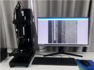
The 14X zoom lens inspection solution is designed to provide a high-resolution, flexible, and efficient solution for wafer inspection by combining a 14X zoom lens with a high-definition industrial camera, built-in coaxial and external ring light, and the POMEAS MetX multi-sensor measurement system.

Wafer Surface Defect Detection
1. Scratch and Crack Detection: Utilizing the high magnification of the 14X zoom lens and the high resolution of the HD industrial camera, scratches and cracks on the wafer surface can be clearly detected at the micron or even nanometer level. The built-in coaxial light and external ring light illumination make these defects present obvious features in the image. POMEAS MetX multi-sensing measurement system analyzes the defects through algorithms and accurately identifies the length, width, depth and other information of the defects and determines the degree of their impact on the wafer's performance.
2. Particle Contaminant Detection: Particle contaminants on the wafer surface, such as dust and metal particles, may affect the electrical performance and yield of the wafer. Ring light can effectively highlight the presence of particles. Through processing and analyzing the image, the system accurately calculates the size, quantity and location of particles, so that the source of contamination can be detected in time and appropriate cleaning and protection measures can be taken.
3. Surface unevenness detection: For the tiny unevenness on the wafer surface caused by process problems, the coaxial light can clearly reflect the changes in its surface contour. The system quantifies the surface flatness deviation through 3D reconstruction and analysis of the image to ensure that the wafer surface meets the requirements of the production process.
Wafer Pattern and Structure Inspection
1. Lithography Pattern Integrity Inspection: In the lithography process of wafer manufacturing, the 14X zoom lens can carry out high magnification observation of the lithography pattern. After the image is captured by the high-definition industrial camera, the MetX system compares the image with the standard pattern to detect whether the pattern integrity, line width, spacing, and other parameters are in accordance with the design requirements, so as to timely detect deviations and defects in the lithography process, and to avoid the adverse effects of the subsequent process. Adverse effects of the subsequent process can be avoided.
2. Chip Structure Size Measurement: Using different magnification of zoom lens, the MetX system can accurately measure various structure sizes of the chip on the wafer, such as transistor size, wiring width, etc. The MetX system realizes sub-micrometer level high-precision measurement through advanced measurement algorithms, which provides key data for the optimization of the performance and quality control of the chip.
Wafer Edge Detection
Edge Defect Detection: Edges of wafers are prone to breakage, chipping and other defects, which affect the subsequent processing and packaging of wafers. By adjusting the angle of the 14X zoom lens and ring light, the edge of the wafer can be fully inspected. The MetX system accurately identifies the type and location of edge defects, preventing defective wafers from entering the next production stage.
Product recommendation
TECHNICAL SOLUTION
MORE+You may also be interested in the following information
FREE CONSULTING SERVICE
Let’s help you to find the right solution for your project!

 ASK POMEAS
  PRICE INQUIRY
  REQUEST DEMO/TEST
  FREE TRIAL UNIT
  ACCURATE SELECTION
 - APPICATION CASE
- RESOURCE CENTER
- DOWNLOAD CENTER
SOLUTIONS SUPPORT
- ZOOM LENS SELECTION TOOL
- TELECENTRIC LENS SELECTION TOOL
- FA LENS SELECTION TOOL
- ZOOM RATIO TABLE
- CERTIFIED MODEL
SELECTION TOOL
- WHY POMEAS
- FAQ
- PRIVACY POLICY
- TERMS OF USE
- DELIVERY & RETURN POLICY
CUSTOMER CARE
 ADDRESS
Add.:No.68, Chongwei Road, Baizhoubian, East district, Dongguan, China, 523000
CONTACT
 Tel:+ 86-0769-2266 0867
 Fax:+ 86-0769-2266 0867
 E-mail:marketing@pomeas.com

Wechat QR code
Software Copyright :2021SR0176001 抄袭必究, 技术支持:誉新源科技