


I. Challenges in Measuring Electroplated Parts:


1. The difficulty of measuring complex shapes and fine structures
Plated components often feature complex geometries (such as curved surfaces, grooves, edges, and deep holes) or intricate structures (like fine threads, precision teeth, and narrow gaps). Traditional tools (such as calipers and micrometers) struggle to access or conform to these areas for measurement, frequently resulting in “unmeasurable” or “inaccurate” readings. For instance, the plated leads of small electronic components (with diameters as small as 0.1–0.5 mm) or curved plated surfaces on automotive parts cannot be accurately captured in their entirety using manual or traditional tools.
2. Three-Dimensional Inspection Requirements for Electroplating Layer Thickness and Surface Quality
One of the core quality indicators in electroplating is coating thickness (e.g., chromium plating thickness must be controlled between 5-20μm), with uniformity being essential (to prevent localized over-thickness or thinness that could lead to corrosion or peeling). Additionally, surfaces may exhibit microscopic defects (e.g., pinholes, bubbles, scratches, pits, potentially only a few micrometers in size). Accurate assessment of these flaws requires three-dimensional topography data (e.g., scratch depth, bubble protrusion height). Traditional 2D measurement tools (e.g., profilometers) cannot capture thickness or three-dimensional information, making it difficult to meet quality requirements.
3. Efficiency and Consistency Issues in Batch Detection
Electroplated parts are typically produced in batches (ranging from thousands to tens of thousands per day). Manual inspection is not only extremely inefficient (with individual measurements potentially taking 1-5 minutes) but also prone to significant error fluctuations influenced by operator experience and fatigue (measurements of the same part by different individuals may vary by more than ±5μm). This makes it difficult to ensure consistent quality across batch production.
4. Surface Reflections and Interference From Contamination
Electroplated surfaces (such as chrome or nickel plating) typically exhibit high gloss, which can cause intense reflections leading to blurred images and edge loss during optical measurement. Additionally, electroplated parts may retain residual electrolyte, moisture, or oil contamination, further interfering with optical imaging and compromising measurement accuracy.
5. The Necessity of Non-Contact Measurement
Electroplated layers are relatively thin (especially decorative plating, such as gold plating which may only be 0.1-1μm thick). Contact measurement methods (such as probes) may scratch the plating or cause part deformation, directly affecting product quality compliance. Therefore, non-contact measurement methods are required.
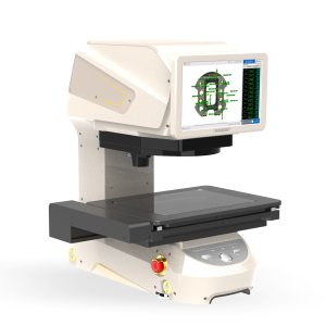
II. Inspection Solution: POMEAS Image Measurement System IMAGE 3 pro-h

1. Addressing Complex Geometries and Fine Structures: Profile Scanning + High-Resolution Optical Systems
The instrument supports contour scanning functionality, enabling continuous scanning of parts through high-precision optical lenses (typically paired with megapixel industrial cameras). This captures complete two-dimensional contour data of curved surfaces, grooves, and minute holes/slits without requiring manual determination of “measurement points,” thereby preventing detail omission. For example, when scanning electroplated parts with deep holes, it can obtain hole wall perpendicularity and diameter variation curves. For micro-pins, it can directly measure diameter, length, and coating coverage integrity.
2. Solving 3D Parametric Measurement: 3D measurement capabilities cover coating thickness and surface defects.
For coating thickness, it can precisely measure micron-level variations (with accuracy up to ±0.1μm) to determine compliance with uniformity requirements. For surface defects (such as scratch depth and bubble height), it quantifies three-dimensional dimensions (e.g., scratch depth of 0.5μm, bubble diameter of 3μm), replacing the subjectivity of manual visual inspection.
3. Enhancing Batch Inspection Efficiency: Mobile Platform + Automated Measurement
Equipped with a 300×200mm movable platform capable of holding multiple small-to-medium plated parts (e.g., electronic connectors, small hardware components) at once. The platform automatically moves and performs sequential measurements, eliminating the need for manual loading and unloading. Additionally, by integrating preset measurement programs (such as one-click access to inspection templates for specific part types), individual measurement time can be reduced to just a few seconds. This significantly boosts batch inspection efficiency while eliminating human operational errors.
4. Optimizing Optical Interference: Anti-Reflection Design and Image Algorithms
The instrument is typically equipped with anti-reflective light sources (such as ring lights or coaxial lights) and image enhancement algorithms to suppress strong reflections on plated surfaces, ensuring sharp edge imaging. For parts contaminated with oil or moisture, image preprocessing techniques (such as deblurring and contrast adjustment) can reduce interference from contaminants, guaranteeing measurement stability.
5. Non-contact Measurement Protection Coating
The entire process employs optical non-contact measurement, avoiding probe contact with the plating surface to prevent scratches or deformation. This makes it particularly suitable for quality inspection of precision decorative plated parts, such as jewelry and high-end instrument housings.
Product recommendation
TECHNICAL SOLUTION
MORE+You may also be interested in the following information
FREE CONSULTING SERVICE
Let’s help you to find the right solution for your project!

 ASK POMEAS
  PRICE INQUIRY
  REQUEST DEMO/TEST
  FREE TRIAL UNIT
  ACCURATE SELECTION
 - APPICATION CASE
- RESOURCE CENTER
- DOWNLOAD CENTER
SOLUTIONS SUPPORT
- ZOOM LENS SELECTION TOOL
- TELECENTRIC LENS SELECTION TOOL
- FA LENS SELECTION TOOL
- ZOOM RATIO TABLE
- CERTIFIED MODEL
SELECTION TOOL
- WHY POMEAS
- FAQ
- PRIVACY POLICY
- TERMS OF USE
- DELIVERY & RETURN POLICY
CUSTOMER CARE
 ADDRESS
Add.:No.68, Chongwei Road, Baizhoubian, East district, Dongguan, China, 523000
CONTACT
 Tel:+ 86-0769-2266 0867
 Fax:+ 86-0769-2266 0867
 E-mail:marketing@pomeas.com

Wechat QR code
Software Copyright :2021SR0176001 抄袭必究, 技术支持:誉新源科技