


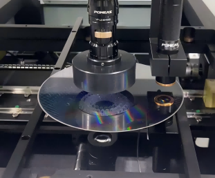
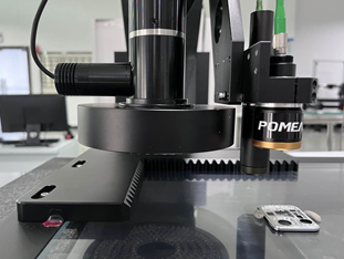
Spectral confocal sensors have become core equipment for industrial precision measurement and quality control due to their non-contact measurement capabilities, nanometer-level high precision, resistance to surface reflection interference, and adaptability to multiple materials. They are widely applied across the following key scenarios:

I. Precision Inspection of Dimensions and Geometric Features
Traditional contact measurement struggles to meet the tolerance requirements of minute, complex components, whereas spectral confocal technology precisely addresses this challenge. In the electronics and semiconductor sector, it can measure circuit board pin pitch ranging from 0.1 to 0.5 mm, semiconductor wafer notch width, and micro-motor shaft diameters between 0.5 and 5 mm. In automotive manufacturing, it detects engine piston skirt roundness ≤5μm and precision guide rail flatness ≤3μm per meter. For consumer electronics and aerospace, it measures ≤0.05mm assembly gaps between phone frames and screens, 0.01-0.1mm step heights on metal parts, and ±2μm tolerances for 2-20mm inner diameters in precision bearings.

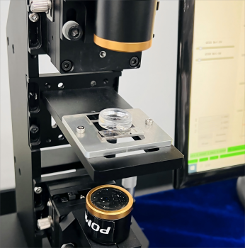
II. Transparent and Multilayer Structure Measurement
Addressing the challenge of multi-interface reflection interference in transparent materials, spectral confocal technology precisely locates interfaces through wavelength resolution. When measuring transparent materials, it can assess the thickness of 0.5-1.2mm smartphone cover glass, 0.3-0.7mm LCD glass substrates, and even 0.1-0.3mm pharmaceutical glass tubes, while simultaneously detecting internal bubbles and impurities. It is compatible with curved components. For multi-layer structures, it enables layered measurement of semiconductor wafer oxide layers (50-500nm), automotive paint multi-layer coatings (50-150μm: electrophoretic layer + midcoat + clearcoat), and PET flexible films (10-50μm) with nanometer-level precision.

III. Surface Quality and Micro-Defect Monitoring
It enables integrated inspection of macro-level contours and micro-level defects: Macroscopically, it measures optical lens curvature radii with ±0.001mm precision, automotive headlight cover surfaces, and mobile phone casing mold cavity surfaces to ensure component assembly compatibility and functional compliance. At the microscopic level, it identifies scratches ≥5nm deep on semiconductor wafers, indentations ≥1μm on metal parts, and pitting ≥20μm on optical glass. It quantifies defect depth and width to meet high-end product quality grading requirements, addressing the shortcomings of traditional visual inspection in detecting minute defects.
IV. Real-Time Monitoring of Dynamic Production Lines
In high-speed continuous production, it works with motion platforms to perform dynamic measurements. For continuous sheet materials, it provides real-time thickness measurement for lithium electrode sheets (50-200μm, ±1μm accuracy) and cold-rolled steel sheets (0.1-2mm) on production lines operating at 1-5m/s. Data is synchronously transmitted to the control system, triggering automatic alarms and parameter adjustments when deviations exceed limits. In automated assembly, it provides ±0.5μm height positioning for semiconductor chip bonding and assists in achieving ≤0.02mm gap alignment for automotive components. Replacing wear-prone mechanical positioning, it enhances assembly precision and stability.
Product recommendation
TECHNICAL SOLUTION
MORE+You may also be interested in the following information
FREE CONSULTING SERVICE
Let’s help you to find the right solution for your project!

 ASK POMEAS
  PRICE INQUIRY
  REQUEST DEMO/TEST
  FREE TRIAL UNIT
  ACCURATE SELECTION
 - APPICATION CASE
- RESOURCE CENTER
- DOWNLOAD CENTER
SOLUTIONS SUPPORT
- ZOOM LENS SELECTION TOOL
- TELECENTRIC LENS SELECTION TOOL
- FA LENS SELECTION TOOL
- ZOOM RATIO TABLE
- CERTIFIED MODEL
SELECTION TOOL
- WHY POMEAS
- FAQ
- PRIVACY POLICY
- TERMS OF USE
- DELIVERY & RETURN POLICY
CUSTOMER CARE
 ADDRESS
Add.:No.68, Chongwei Road, Baizhoubian, East district, Dongguan, China, 523000
CONTACT
 Tel:+ 86-0769-2266 0867
 Fax:+ 86-0769-2266 0867
 E-mail:marketing@pomeas.com

Wechat QR code
Software Copyright :2021SR0176001 抄袭必究, 技术支持:誉新源科技