


Testing Background:

As the core substrate for semiconductor devices, the surface flatness and defect control of wafers directly determine chip yield and performance. Microscopic defects such as particles, scratches, and pits (typically ranging from nanometers to micrometers in size) cannot be accurately assessed for their impact on device integrity through 2D optical inspection alone.
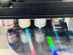
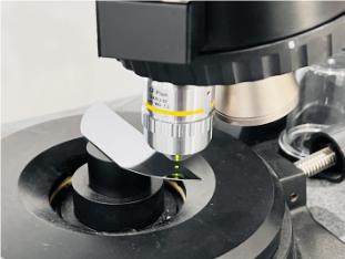
Inspection Solution: POMEAS White Light Interferometric Profiler

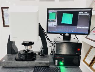
Using non-contact 3D profile measurement technology, the white light interferometer converts these invisible or minute defects into precise 3D quantitative data—including defect volume, depth/height, and cross-sectional profiles—providing engineers with critical evidence to trace defect origins, assess performance impacts, and optimize manufacturing processes.

The quantitative capability of optical interferometers stems from their unique interferometric imaging mechanism: white light emitted by the device is split into two beams by a beam splitter. One beam illuminates the wafer surface (measurement beam), while the other illuminates a standard reference plane (reference beam). After reflection, the two beams recombine to form interference fringes. The brightness variations in these fringes directly correlate with the phase difference, which in turn reflects the height difference between the wafer surface and the reference plane.
By scanning the wafer surface point-by-point along the Z-axis, collecting interference signals from different positions, and reconstructing them through algorithms, a 3D topographic map covering the inspection area is generated. This transforms abstract surface defects into quantifiable three-dimensional data. Compared to traditional 2D inspection, which only captures the planar dimensions of defects, the 3D quantification of the white light interferometer fully reveals the spatial morphology of defects—a critical factor in assessing their severity.
Product recommendation
TECHNICAL SOLUTION
MORE+You may also be interested in the following information
FREE CONSULTING SERVICE
Let’s help you to find the right solution for your project!

 ASK POMEAS
  PRICE INQUIRY
  REQUEST DEMO/TEST
  FREE TRIAL UNIT
  ACCURATE SELECTION
 - APPICATION CASE
- RESOURCE CENTER
- DOWNLOAD CENTER
SOLUTIONS SUPPORT
- ZOOM LENS SELECTION TOOL
- TELECENTRIC LENS SELECTION TOOL
- FA LENS SELECTION TOOL
- ZOOM RATIO TABLE
- CERTIFIED MODEL
SELECTION TOOL
- WHY POMEAS
- FAQ
- PRIVACY POLICY
- TERMS OF USE
- DELIVERY & RETURN POLICY
CUSTOMER CARE
 ADDRESS
Add.:No.68, Chongwei Road, Baizhoubian, East district, Dongguan, China, 523000
CONTACT
 Tel:+ 86-0769-2266 0867
 Fax:+ 86-0769-2266 0867
 E-mail:marketing@pomeas.com

Wechat QR code
Software Copyright :2021SR0176001 抄袭必究, 技术支持:誉新源科技