


How does metallographic microscopy reveal microcracks, hole wall tears, and plating voids in PCB?
Testing Background:

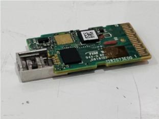
Printed circuit boards (PCBs) serve as the core structural components of electronic devices, with the integrity of their microscopic internal structures directly determining device reliability. Common defects such as microcracks, hole wall tears, and plating voids are typically micrometer-scale, concealed within the substrate or hole walls. Conventional inspection methods struggle to accurately identify these flaws, yet they can trigger critical failures like signal anomalies and short circuits.
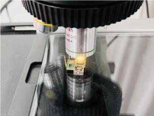
Solution: POMEAS Metallographic Microscope
Metallographic microscopes, with their high magnification capabilities ranging from 500X to 1000X, clearly reveal the morphology and distribution of various microscopic defects, making them indispensable core equipment in PCB quality inspection.

For resin microcracks, high magnification clearly reveals linear dark fissures measuring 1-5 micrometers, precisely identifying their initiation points and propagation directions—a level of localization and analysis unattainable through low magnification or ultrasonic testing. For hole wall tears and drilling burrs, 1000X magnification clearly reveals the jagged morphology of torn glass fibers, enabling identification of burr material and dimensions. This provides direct evidence for optimizing drilling processes, outperforming low-magnification optical observation and X-ray inspection.

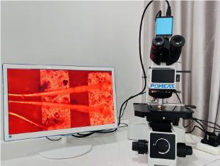
During chemical copper plating and electroplating processes, metallographic microscopes can precisely capture latent defects such as discontinuities and pinholes in the copper deposit layer, as well as circular voids measuring 2–8 micrometers within the plating layer. They can also correlate these defects with their root causes (e.g., aged copper plating solution, uneven current distribution). Conventional conductivity testing or ultrasonic scanning can only assess macro-level compliance, failing to visualize or trace microscopic defects.
Product recommendation
TECHNICAL SOLUTION
MORE+You may also be interested in the following information
FREE CONSULTING SERVICE
Let’s help you to find the right solution for your project!

 ASK POMEAS
  PRICE INQUIRY
  REQUEST DEMO/TEST
  FREE TRIAL UNIT
  ACCURATE SELECTION
 - APPICATION CASE
- RESOURCE CENTER
- DOWNLOAD CENTER
SOLUTIONS SUPPORT
- ZOOM LENS SELECTION TOOL
- TELECENTRIC LENS SELECTION TOOL
- FA LENS SELECTION TOOL
- ZOOM RATIO TABLE
- CERTIFIED MODEL
SELECTION TOOL
- WHY POMEAS
- FAQ
- PRIVACY POLICY
- TERMS OF USE
- DELIVERY & RETURN POLICY
CUSTOMER CARE
 ADDRESS
Add.:No.68, Chongwei Road, Baizhoubian, East district, Dongguan, China, 523000
CONTACT
 Tel:+ 86-0769-2266 0867
 Fax:+ 86-0769-2266 0867
 E-mail:marketing@pomeas.com

Wechat QR code
Software Copyright :2021SR0176001 抄袭必究, 技术支持:誉新源科技