


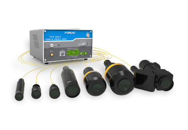
Spectral Sensor Application for Transparent Object Thickness Measurement
For measuring the total thickness and layer thickness of transparent materials (glass, film), spectral confocal technology achieves high-precision, non-contact detection through various configuration solutions.

I. Single-Point Solution: Thickness Measurement Based on Refractive Index Compensation
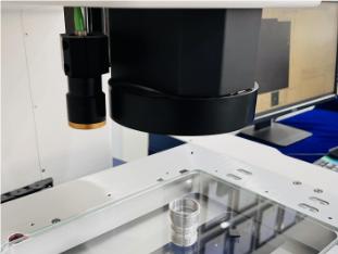
1. Technical Principle: The single-side single-point solution emits polychromatic light through a single probe. Leveraging the “wavelength-displacement linear mapping” characteristic of spectral confocal imaging, it captures the characteristic wavelengths of reflected light from the upper and lower surfaces of transparent objects. Combined with material refractive index calculations, this determines the total thickness. The core formula is: D = 2⋅Δλ/ΔD(λ2 − λ1)⋅n
Where λ1 and λ2 represent the wavelengths of reflected light from the upper and lower surfaces, respectively; n denotes the material refractive index; and Δλ/ΔD is the sensor wavelength-displacement calibration coefficient.
2. Key Advantages:
(1) Non-contact measurement: Eliminates damage to flexible films caused by contact tools (e.g., micrometers), particularly suitable for ultra-thin materials (e.g., 50μm PET film);
(2) Single-side operation: Requires illumination from only one side, suitable for enclosed spaces or inaccessible scenarios (e.g., internal structure inspection of mobile phone screens);
(3) High precision: Resolution up to 0.1μm, meeting the curved glass thickness tolerance requirement of ≤±10μm in the 3C electronics industry.
3. Typical Application Scenarios: Single-layer glass thickness inspection, film layer thickness monitoring.
II. Bilateral Synchronous Approach: Absolute Thickness Measurement Based on Optical Path Difference

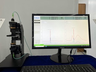
1. Technical Principle: The bilateral synchronous approach employs two sensors positioned opposite each other to measure the propagation path lengths of light through the upper and lower surfaces of a transparent object. The geometric thickness is directly calculated from the optical path difference using the formula: D = (L₂ − L₁)/2. Here, L₁ and L₂ represent the distances from each sensor to the upper and lower surfaces, respectively. This method does not rely on refractive index and achieves nanometer-level precision.
2. Key Advantages:
(1) Absolute Accuracy: Eliminates refractive index errors, particularly suitable for high-refractive-index materials (e.g., sapphire, n=1.77) or composite materials (e.g., glass + ceramic coating).
(2) Dynamic Measurement: Supports high-speed object detection, such as thickness fluctuation monitoring during semiconductor wafer transport.
(3) Wide Coverage: Expands the measurement area through XY-axis motion platforms, enabling full inspection of large transparent objects (e.g., display panel glass).
3. Typical Application Scenarios: Semiconductor wafer thickness inspection, aerospace transparent component inspection.
III. Selection Recommendations
- For detecting single-layer glass or multilayer films with known refractive indices under budget constraints, prioritize the single-side single-point solution.
- For measuring high-refractive-index materials, composites, or large transparent objects with stringent accuracy requirements, the dual-side simultaneous solution is the optimal choice.
Product recommendation
TECHNICAL SOLUTION
MORE+You may also be interested in the following information
FREE CONSULTING SERVICE
Let’s help you to find the right solution for your project!

 ASK POMEAS
  PRICE INQUIRY
  REQUEST DEMO/TEST
  FREE TRIAL UNIT
  ACCURATE SELECTION
 - APPICATION CASE
- RESOURCE CENTER
- DOWNLOAD CENTER
SOLUTIONS SUPPORT
- ZOOM LENS SELECTION TOOL
- TELECENTRIC LENS SELECTION TOOL
- FA LENS SELECTION TOOL
- ZOOM RATIO TABLE
- CERTIFIED MODEL
SELECTION TOOL
- WHY POMEAS
- FAQ
- PRIVACY POLICY
- TERMS OF USE
- DELIVERY & RETURN POLICY
CUSTOMER CARE
 ADDRESS
Add.:No.68, Chongwei Road, Baizhoubian, East district, Dongguan, China, 523000
CONTACT
 Tel:+ 86-0769-2266 0867
 Fax:+ 86-0769-2266 0867
 E-mail:marketing@pomeas.com

Wechat QR code
Software Copyright :2021SR0176001 抄袭必究, 技术支持:誉新源科技