


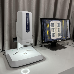
In recent years, motorized zoom microscopes have gradually become essential equipment in semiconductor inspection. By replacing traditional manual zoom and focusing with motorized drives, and integrating automatic illumination and image processing, these microscopes aim to address the inspection challenges posed by shrinking chip sizes and increasingly complex structures.

1. What are its components?
At the heart of an electric zoom microscope is an electronically controlled optical system, which performs inspection tasks through the coordinated operation of the following components:
-
Motorized Zoom and Focus Module: This is the device’s actuator. Stepper motors or servo motors directly drive the optical lens assembly along guide rails to switch magnification levels and adjust the focal length. By eliminating the mechanical linkages and cams associated with manual operation, the electronic control system achieves higher positioning accuracy and can precisely reproduce specific magnification levels and focal plane positions. In practice, this means that with a single click of a button, the device automatically switches to preset observation conditions.
-
Programmable LED Illumination: Since semiconductor materials exhibit varying surface reflectivity, illumination must be flexibly adjusted. A common configuration involves integrated multi-channel LED light sources, such as ring or spot illumination, where the brightness and on/off status of each channel can be controlled independently. Operators can save different illumination profiles for various sample types—such as highly reflective metal layers or transparent photoresists—and the system will automatically restore these optical settings when the profile is recalled.
2. What issues does it address in the testing process?
Based on feedback from actual production lines, this type of equipment has been adopted primarily because it addresses several specific pain points:
-
Reducing operator-induced variations: With manual microscopes, differences in zoom force, focusing habits, and lighting preferences among operators can all affect observation results, which can easily lead to disputes during process re-inspection or failure analysis. With motorization, observation parameters are standardized; regardless of who is operating the microscope, as long as the same program is used, the field of view and results will be consistent, providing a stable baseline for subsequent measurements and evaluations.
-
Improving the Efficiency of Repetitive Inspections: On semiconductor production lines, it is often necessary to perform periodic spot checks at fixed locations on the same batch of wafers. Manual operations require repeatedly locating the field of view and adjusting the focus, which is time-consuming and tedious. Motorized microscopes can automatically locate previously inspected positions using coordinate-based positioning, automatically focus, and switch to preset magnifications. Operators need only observe and make judgments, eliminating the need for repeated adjustments.
-
Expanding the inspection scope of a single device: A single chip varies greatly in size, ranging from its external packaging to its internal circuitry. In the past, it might have been necessary to first use a stereo microscope to view the overall structure, then switch to a metallurgical microscope to examine the details. An electric zoom system allows for continuous magnification adjustment over a wide range, enabling a single device to meet the needs of both low-magnification overview inspections and high-magnification detailed observations, thereby eliminating the hassle of transferring samples between different devices.
3. What are its main applications in semiconductor manufacturing?
Currently, this type of equipment is primarily used in the following areas:
-
Process monitoring in wafer fabrication: Following processes such as lithography, etching, and cleaning, this step involves spot-checking the wafer surface for foreign particles, scratches, pattern defects, and other issues.
-
Quality Inspection for Packaging and Dicing: After chip dicing, mounting, and wire bonding, the interior of the package must be inspected for cracks, and the wires must be checked for sagging or breaks.
-
Failure Analysis Localization: When a chip fails, the first step is to use a microscope to precisely locate the failure site and take photographs for documentation, either without opening the package or with it partially opened.
Product recommendation
TECHNICAL SOLUTION
MORE+You may also be interested in the following information
FREE CONSULTING SERVICE
Let’s help you to find the right solution for your project!

 ASK POMEAS
  PRICE INQUIRY
  REQUEST DEMO/TEST
  FREE TRIAL UNIT
  ACCURATE SELECTION
 - APPICATION CASE
- RESOURCE CENTER
- DOWNLOAD CENTER
SOLUTIONS SUPPORT
- ZOOM LENS SELECTION TOOL
- TELECENTRIC LENS SELECTION TOOL
- FA LENS SELECTION TOOL
- ZOOM RATIO TABLE
- CERTIFIED MODEL
SELECTION TOOL
- WHY POMEAS
- FAQ
- PRIVACY POLICY
- TERMS OF USE
- DELIVERY & RETURN POLICY
CUSTOMER CARE
 ADDRESS
Add.:No.68, Chongwei Road, Baizhoubian, East district, Dongguan, China, 523000
CONTACT
 Tel:+ 86-0769-2266 0867
 Fax:+ 86-0769-2266 0867
 E-mail:marketing@pomeas.com

Wechat QR code
Software Copyright :2021SR0176001 抄袭必究, 技术支持:誉新源科技