


In the field of electronics manufacturing, printed circuit boards (PCBs) serve as the carriers for electronic components. Their dimensional accuracy and geometric tolerances directly impact the performance and stability of entire electronic products. As electronic devices trend toward miniaturization and higher integration, PCB designs grow increasingly complex and larger in size, placing higher demands on measurement technology. Particularly today, when PCB lengths commonly reach around 200mm, traditional measurement equipment struggles to achieve precise, single-pass measurement of entire PCBs due to their limited field of view (typically under φ100mm). This has led to the emergence of large-field-of-view stitching measurement technology as the key solution to this challenge.

What is Wide-View Stitch Measurement?

Wide-Field Stitching Measurement is an advanced image measurement technology that intelligently stitches multiple small-field measurement images to form a high-precision measurement image covering a larger area. This enables comprehensive and accurate measurement of large-sized workpieces. This technology not only overcomes the limited field-of-view drawbacks of traditional measurement equipment but also maintains the high precision and efficiency of image measurement. It is particularly suitable for scenarios requiring high-precision, large-area measurement, such as PCB boards.
During PCB measurement, complex board layouts, dense component placement, and multiple critical dimensions requiring simultaneous measurement—such as hole spacing, trace width, and board edge profiles—pose significant challenges. Traditional measurement methods either require multiple repositionings of the workpiece or measuring head—a time-consuming and error-prone process—or fail to capture complete measurement data in a single pass due to insufficient field of view. Wide-field stitching measurement technology, however, seamlessly combines images captured from multiple angles through automated or semi-automated processes. This creates a single comprehensive image encompassing all critical measurement points, significantly enhancing both measurement accuracy and efficiency.
Wide-Field Stitching Applications in PCB Board Measurement
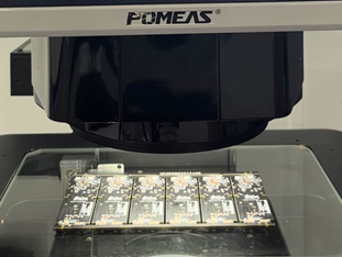
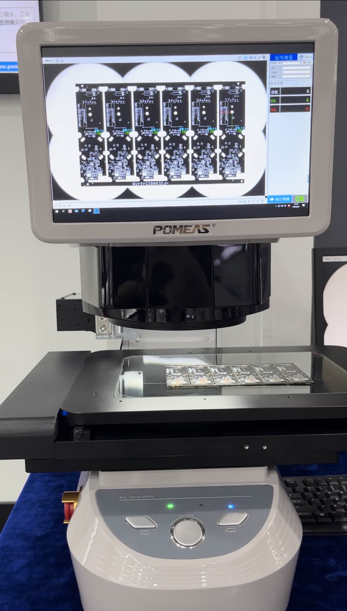
Taking a 200mm-long PCB board as an example, conventional measurement equipment may require multiple measurements with manual data stitching. This process is not only cumbersome but also prone to inaccuracies in the final assembly. In contrast, employing wide-field stitching measurement technology allows the PCB board to be placed on the measurement platform. The imaging measurement system automatically scans and stitches the images, enabling the acquisition of precise measurement data for the entire board in a single pass. This includes, but is not limited to, critical metrics such as hole position accuracy, trace spacing, and board flatness, providing robust support for PCB quality control.
Advantages of the POMEAS Image3 Pro High-Precision Image Measuring Instrument

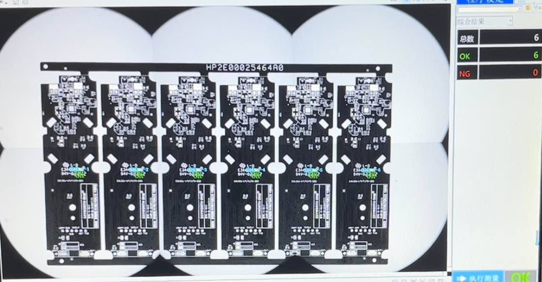
Among numerous image measurement instruments, the POMEAS Image3 Pro high-precision image measurement system stands out for its exceptional wide-field stitching measurement capabilities. Utilizing advanced image processing algorithms and a high-precision optical system, the Image3 Pro achieves rapid and accurate wide-field image stitching, effortlessly handling even complex and varied PCB boards. Its advantages include:
1. High-Precision Measurement: Utilizes sub-pixel image processing technology to ensure micron-level accuracy in measurement results, meeting the stringent dimensional precision requirements of PCB boards.
2. Wide-Field Stitching: Supports automatic stitching of multiple images to cover a larger measurement area, eliminating the need for repeated workpiece repositioning and enhancing measurement efficiency.
3. Intelligent Recognition and Measurement: Built-in AI recognition software automatically identifies critical measurement points on PCBs, reducing manual intervention and enhancing measurement accuracy.
4. User-Friendly Operation: An intuitive interface and one-click workflow enable quick mastery even by non-specialists, lowering the learning curve.
5. Data Management and Analysis: Provides robust data management and analysis capabilities, supporting measurement data export, comparison, and report generation to empower enterprises in achieving quality traceability and continuous improvement.
Product recommendation
TECHNICAL SOLUTION
MORE+You may also be interested in the following information
FREE CONSULTING SERVICE
Let’s help you to find the right solution for your project!

 ASK POMEAS
  PRICE INQUIRY
  REQUEST DEMO/TEST
  FREE TRIAL UNIT
  ACCURATE SELECTION
 - APPICATION CASE
- RESOURCE CENTER
- DOWNLOAD CENTER
SOLUTIONS SUPPORT
- ZOOM LENS SELECTION TOOL
- TELECENTRIC LENS SELECTION TOOL
- FA LENS SELECTION TOOL
- ZOOM RATIO TABLE
- CERTIFIED MODEL
SELECTION TOOL
- WHY POMEAS
- FAQ
- PRIVACY POLICY
- TERMS OF USE
- DELIVERY & RETURN POLICY
CUSTOMER CARE
 ADDRESS
Add.:No.68, Chongwei Road, Baizhoubian, East district, Dongguan, China, 523000
CONTACT
 Tel:+ 86-0769-2266 0867
 Fax:+ 86-0769-2266 0867
 E-mail:marketing@pomeas.com

Wechat QR code
Software Copyright :2021SR0176001 抄袭必究, 技术支持:誉新源科技