


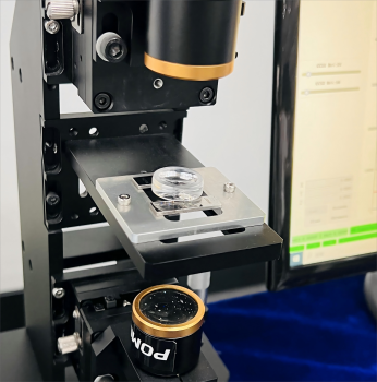
Case Study: Spectral Confocal Displacement Sensors—Solutions for Semiconductor, Glass Thickness, etc
In the field of industrial inspection, accuracy and adaptability are often viewed as two qualities that are difficult to achieve simultaneously. While traditional contact-based measurement offers stable accuracy, it is limited by material constraints and is subject to mechanical wear; conversely, while non-contact optical measurement is highly efficient, it often struggles with transparent materials and highly reflective surfaces. Spectral confocal displacement sensors resolve this contradiction through their unique spectral separation principle.

The core features of this technology can be summarized by four “no's”: non-contact—preventing damage to both the workpiece and the probe; non-discriminatory—enabling stable measurements across a wide range of surfaces, from mirror-like to diffuse reflection, and from transparent to dark; unrestricted—combining nanometer-level resolution with millimeter-level measurement range, covering both microstructures and large-scale topographies; Unsensitive—it exhibits strong resistance to environmental disturbances such as temperature fluctuations and stray light, making it suitable for long-term deployment in industrial settings.
At the inspection solution level, these characteristics translate into significant advantages. First, it can accurately map complex surfaces, such as lens surfaces, microgrooves, and steep-sloped structures, filling the blind spots of traditional sensors in such scenarios. Second, leveraging its spectral resolution capabilities at different material interfaces, it enables thickness measurement of transparent materials and multilayer structures without changing probes or altering the optical path, significantly improving inspection efficiency. Furthermore, since the measurement process is non-contact and wear-free, the system offers higher long-term stability and lower overall operating costs.
In terms of practical applications, spectral confocal displacement sensors have become the “standard equipment” in multiple high-precision manufacturing sectors. In semiconductor inspection, they are used to measure wafer surface microstructures, coating thicknesses, and hidden cutting grooves; in the glass and display industries, they perform online monitoring of flat glass, curved cover plates, bonding adhesive layers, and OLED multilayer film thicknesses; In precision component inspection, they verify the dimensions and contours of micro-motor parts, precision connectors, and microstructures in medical devices; in surface profile scanning and various high-precision industrial measurement solutions, they are gradually becoming the preferred core measurement module for integrators due to their excellent angular adaptability and material compatibility.
For inspection equipment, the introduction of spectral confocal technology represents not merely a sensor upgrade, but a complete overhaul of overall capabilities. It significantly enhances the measurement accuracy and inspection efficiency of equipment, enabling it to handle more challenging inspection tasks; it eliminates the risk of secondary errors caused by mechanical probes through a non-contact approach, thereby improving data authenticity and repeatability; more importantly, it extends the application scope of inspection equipment from traditional metal processing to cutting-edge industries such as semiconductors, optoelectronics, and new energy, endowing inspection equipment with stronger market competitiveness and a technological moat.
Product recommendation
TECHNICAL SOLUTION
MORE+You may also be interested in the following information
FREE CONSULTING SERVICE
Let’s help you to find the right solution for your project!

 ASK POMEAS
  PRICE INQUIRY
  REQUEST DEMO/TEST
  FREE TRIAL UNIT
  ACCURATE SELECTION
 - APPICATION CASE
- RESOURCE CENTER
- DOWNLOAD CENTER
SOLUTIONS SUPPORT
- ZOOM LENS SELECTION TOOL
- TELECENTRIC LENS SELECTION TOOL
- FA LENS SELECTION TOOL
- ZOOM RATIO TABLE
- CERTIFIED MODEL
SELECTION TOOL
- WHY POMEAS
- FAQ
- PRIVACY POLICY
- TERMS OF USE
- DELIVERY & RETURN POLICY
CUSTOMER CARE
 ADDRESS
Add.:No.68, Yongwei Road, Baizhoubian, Dongcheng District, Dongguan, China,523000
CONTACT
 Tel:+ 86-0769-2266 0867
 Fax:+ 86-0769-2266 0867
 E-mail:marketing@pomeas.com

Wechat QR code
Software Copyright :2021SR0176001 抄袭必究, 技术支持:誉新源科技