


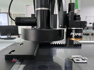
Non-contact measurement solution: Spectral confocal displacement sensor
In the fields of high-end manufacturing and precision inspection, the ability to perform sub-micron measurements of complex surfaces, transparent materials, and even multi-layer structures without coming into contact with the workpiece has always been a key technical challenge. Spectral confocal displacement sensors offer the ideal solution to this challenge thanks to their unique optical principles.

In terms of its characteristics, this technology demonstrates superior performance across multiple dimensions. Its high resolution easily reaches the nanometer level, while its wide dynamic range allows for the simultaneous measurement of both microscopic contours and macroscopic topography within a single device. Non-contact measurement fundamentally eliminates the risk of scratches or probe wear associated with traditional contact probes. More importantly, it provides stable performance on a wide range of surface materials—including mirror-like, transparent, absorptive, and rough surfaces—and offers strong resistance to environmental interference. It is insensitive to temperature drift and changes in ambient lighting, making it suitable for deployment in complex production line environments.

The advantages of this technology are further amplified in inspection applications. It can accurately reproduce complex surfaces such as curved surfaces, steep slopes, and fine grooves; for transparent or multilayer materials, it utilizes spectral information reflected at different interfaces to enable simultaneous measurement of multiple layers using a single probe. The entire process is efficient and stable, and because it requires no mechanical contact, it significantly reduces probe wear and maintenance costs, making it particularly suitable for continuous mass production scenarios.
In practical applications, spectral confocal displacement sensors have become widely adopted in numerous high-tech fields:
-
In semiconductor inspection, for measuring wafer warpage and coating thickness;
-
In glass processing, it precisely controls the thickness of cover glass and multi-layer laminated structures in displays;
-
In precision component inspection, it performs contour scanning of micro-gears and metal structural parts;
-
In surface contour scanning and various high-precision industrial measurement solutions, it is gradually becoming the core sensing unit that replaces traditional laser triangulation or contact-based measurement methods.
POMEAS’ proprietary spectral confocal displacement sensor not only takes inspection equipment to the next level in terms of accuracy and efficiency, but also enhances the reliability of measurement results by eliminating contact-based errors. At the same time, it significantly expands the application scope of inspection equipment, providing reliable quality monitoring methods for previously difficult-to-inspect transparent materials, highly reflective components, and multi-layer composite structures, thereby laying a more solid data foundation for smart manufacturing.
Product recommendation
TECHNICAL SOLUTION
MORE+You may also be interested in the following information
FREE CONSULTING SERVICE
Let’s help you to find the right solution for your project!

 ASK POMEAS
  PRICE INQUIRY
  REQUEST DEMO/TEST
  FREE TRIAL UNIT
  ACCURATE SELECTION
 - APPICATION CASE
- RESOURCE CENTER
- DOWNLOAD CENTER
SOLUTIONS SUPPORT
- ZOOM LENS SELECTION TOOL
- TELECENTRIC LENS SELECTION TOOL
- FA LENS SELECTION TOOL
- ZOOM RATIO TABLE
- CERTIFIED MODEL
SELECTION TOOL
- WHY POMEAS
- FAQ
- PRIVACY POLICY
- TERMS OF USE
- DELIVERY & RETURN POLICY
CUSTOMER CARE
 ADDRESS
Add.:No.68, Yongwei Road, Baizhoubian, Dongcheng District, Dongguan, China,523000
CONTACT
 Tel:+ 86-0769-2266 0867
 Fax:+ 86-0769-2266 0867
 E-mail:marketing@pomeas.com

Wechat QR code
Software Copyright :2021SR0176001 抄袭必究, 技术支持:誉新源科技