


In the electronics manufacturing industry, the soldering quality of FPGA (Field-Programmable Gate Array) chips directly determines the performance and reliability of the entire circuit board. As the trend toward component miniaturization intensifies, detecting defects such as solder bump height, coplanarity, and the pillow effect has become increasingly challenging. Thanks to their non-contact, high-precision, and high-speed capabilities, 3D line laser profilometers have become the ideal solution for FPGA solder bump quality control.

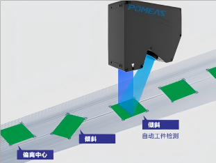
I. Core Principle: 3D Reconstruction Based on Laser Triangulation

The operating principle of 3D line laser profilometers is based on the classic laser triangulation method. This system typically consists of a high-precision laser and a sensitive CMOS/CCD image sensor. The workflow primarily involves the following three steps:
1. Laser Line Projection: A laser diode inside the sensor uses a special lens to expand the point light source into a stable, uniform, static laser line, which is projected vertically or at an angle onto the surface of the FPGA chip and PCB board.
2. Diffuse Reflection Capture: When the laser line strikes the surfaces of objects at different heights (such as the tops of solder balls, the chip body, or the PCB substrate), diffuse reflection occurs. The reflected light passes through a high-quality optical system and is imaged onto the image sensor.
3. Height Calculation: When the surface height of an object changes (e.g., from the substrate to the top of a solder ball), the position of the reflected light on the sensor chip shifts. Built-in algorithms rapidly calculate the actual height (Z-axis coordinate) of that point based on trigonometric relationships. Simultaneously, as the conveyor belt moves or the sensor performs lateral scanning, X- and Y-axis data are acquired, ultimately synthesizing a complete 3D profile.
II. Advantages of 3D Line Laser Profile Sensors

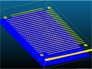
1. Precise Co-planarity Measurement: FPGAs typically use BGA (Ball Grid Array) or LGA (Land Grid Array) packaging. The sensor can scan an entire row of solder joints in a single pass. By capturing the 3D coordinates of each solder joint, it accurately calculates the maximum, minimum, and average heights of the solder joints, thereby determining whether there is a risk of lifted pins or cold solder joints.
2. Detection of the “Pillow Effect”: When solder does not melt sufficiently, the solder ball and pad appear to be in contact but are actually separated, creating the so-called “pillow effect.” 2D vision struggles to detect such defects, whereas 3D sensors can effectively capture these subtle anomalies by analyzing the three-dimensional shape and sudden changes in solder joint height.
3. Adapting to Reflective and Multi-Material Surfaces: FPGA chip packages typically feature a black solder mask, while solder joints have a metallic sheen. Traditional sensors are prone to overexposure or data loss when encountering mirror-like reflections. High-quality 3D line laser profilometers, equipped with advanced exposure algorithms and filtering techniques, can simultaneously handle both matte and highly reflective surfaces, ensuring data integrity.
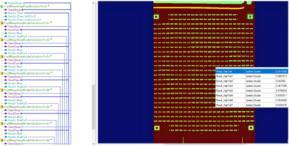
III. Practical Application: FPGA Solder Joint Height Inspection Solution

1. Dynamic Scanning:
The FPGA carrier board moves at a constant speed beneath the sensor, which captures thousands to tens of thousands of contour lines per second to ensure no data is missed.
2. Data Alignment and Filtering:
The system preprocesses the raw point cloud data to remove noise interference and calibrates it using a reference plane (such as the PCB surface).
3. Feature Extraction and Classification:
- Height Measurement: Extracts the peak height of the solder joint area and compares it to preset upper and lower threshold limits.
- Volume Estimation: Based on continuous contour lines, the system can approximate the volume of solder paste or the solder joint, thereby indirectly determining whether the amount of solder is sufficient.
- Defect Marking: If the height of a solder joint is significantly lower than that of adjacent joints, or if there are abnormal fluctuations in overall height, the system immediately identifies it as a defect and marks its coordinates.
Product recommendation
TECHNICAL SOLUTION
MORE+You may also be interested in the following information
FREE CONSULTING SERVICE
Let’s help you to find the right solution for your project!

 ASK POMEAS
  PRICE INQUIRY
  REQUEST DEMO/TEST
  FREE TRIAL UNIT
  ACCURATE SELECTION
 - APPICATION CASE
- RESOURCE CENTER
- DOWNLOAD CENTER
SOLUTIONS SUPPORT
- ZOOM LENS SELECTION TOOL
- TELECENTRIC LENS SELECTION TOOL
- FA LENS SELECTION TOOL
- ZOOM RATIO TABLE
- CERTIFIED MODEL
SELECTION TOOL
- WHY POMEAS
- FAQ
- PRIVACY POLICY
- TERMS OF USE
- DELIVERY & RETURN POLICY
CUSTOMER CARE
 ADDRESS
Add.:No.68, Chongwei Road, Baizhoubian, East district, Dongguan, China, 523000
CONTACT
 Tel:+ 86-0769-2266 0867
 Fax:+ 86-0769-2266 0867
 E-mail:marketing@pomeas.com

Wechat QR code
Software Copyright :2021SR0176001 抄袭必究, 技术支持:誉新源科技