


Inspection of Diode Appearance and Physical Properties

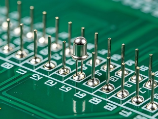
1. Visual Integrity: Inspect the package for damage, cracks, scratches, bubbles, foreign objects, deformation, oxidation, or burn marks, and verify that surface markings are clear and legible.
2. Dimensional Accuracy: Measure the chip size, electrode spacing, pin spacing, pin coplanarity, and surface flatness to ensure compliance with design tolerances.
3. Structural Defects: Use microscopy or X-ray imaging to inspect the interior of the package for voids, delamination, chip cracks, broken bond wires, and detached solder joints.
Advantages of ZOOM LENSes in LED Inspection

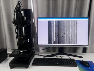
1. Multi-scale inspection capability: A single lens enables continuous zoom from low magnification to high magnification. During inspection, users can first use a low magnification (e.g., 0.7x) to quickly scan the entire diode or a full tray of components to locate suspicious areas; then, with a single click, switch to high magnification (e.g., 7x or higher) for microscopic observation of pin soldering, fine scratches, and foreign objects on the chip surface.
2. Enhanced Inspection Efficiency and Flexibility: The motorized ZOOM LENS completes magnification switching in 0.5 seconds, which is several times faster than manual zooming or changing fixed-magnification lenses. When dealing with different diode package types (such as SOD, SMA, DO-35, etc.), simply call up pre-set magnification parameters and inspection programs in the software. This reduces production line changeover time from several hours to just a few minutes, significantly improving equipment utilization rates.
3. Balancing Resolution and Depth of Field: Traditional high-magnification lenses have an extremely narrow depth of field, making it difficult to simultaneously capture clear images of certain aspects of diode structures with varying heights (such as lead bend height, the stepped surface of the plastic package, and the coplanarity of solder balls). ZOOM LENSes allow selection of a moderate magnification, providing a greater depth of field while ensuring sufficient resolution. This keeps features clear across the entire height range, facilitating the detection of three-dimensional defects.
4. High-Quality Imaging Combined with Lighting: Modern 4K-class ZOOM LENSes achieve a resolution of approximately 2.8 μm on the object side, enabling clear identification of minute defects such as solder joint oxidation layers, tiny air bubbles, and electrode scratches. When combined with coaxial incident illumination, they can effectively suppress glare from diode leads or chip surfaces, rendering fine scratches and foreign objects with greater sharpness. Additionally, the modular design allows ZOOM LENSes to be easily paired with various illumination methods—such as ring lighting, backlighting, and polarized light—to meet the inspection requirements of different materials.
5. Easy system integration: ZOOM LENSes typically use standard mounts (such as the C-mount), allowing for quick compatibility with mainstream industrial cameras. When paired with an autofocus module, they enable fully automatic real-time focusing and zooming, seamlessly integrating into in-line inspection equipment to meet the continuous operation requirements of high-speed production lines.
Product recommendation
TECHNICAL SOLUTION
MORE+You may also be interested in the following information
FREE CONSULTING SERVICE
Let’s help you to find the right solution for your project!

 ASK POMEAS
  PRICE INQUIRY
  REQUEST DEMO/TEST
  FREE TRIAL UNIT
  ACCURATE SELECTION
- APPICATION CASE
- RESOURCE CENTER
- DOWNLOAD CENTER
SOLUTIONS SUPPORT
- ZOOM LENS SELECTION TOOL
- TELECENTRIC LENS SELECTION TOOL
- FA LENS SELECTION TOOL
- ZOOM RATIO TABLE
- CERTIFIED MODEL
SELECTION TOOL
- WHY POMEAS
- FAQ
- PRIVACY POLICY
- TERMS OF USE
- DELIVERY & RETURN POLICY
CUSTOMER CARE
 ADDRESS
Add.:No.68, Yongwei Road, Baizhoubian, Dongcheng District, Dongguan, China,523000
CONTACT
 Tel:+ 86-0769-2266 0867
 Fax:+ 86-0769-2266 0867
 E-mail:marketing@pomeas.com

Wechat QR code

Software Copyright :2021SR0176001 抄袭必究, 技术支持:誉新源科技