


From Contours to Defects: Applications of Line Laser Profile Sensors
When introducing automated inspection equipment, many manufacturing companies often face a dilemma: while 2D cameras can detect most surface defects, certain defects related to “height”—such as breaks in adhesive dispensing paths, bent battery tabs, and loose screws—remain difficult to identify effectively. These defects cannot be detected solely through grayscale image recognition; accurate detection requires the use of 3D contour data.

The value of a line laser profile sensor lies in its ability to expand the detection dimension from two dimensions to three. It not only outputs a simple profile line but also analyzes profile features through algorithms to directly determine dimensional compliance and defect types. Below are examples of its practical application in several typical scenarios.
Scenario 1: Dispensing and Adhesive Path Inspection

In processes such as adhesive dispensing on mobile phone frames and chip underfill, the height, width, and continuity of the adhesive bead directly affect bonding strength and insulation performance. The line laser profile sensor scans at high speed along the adhesive path to capture the cross-sectional profile of the adhesive in real time. By utilizing preset height thresholds and width ranges, the system can automatically detect defects such as adhesive breaks, sagging, and out-of-tolerance widths, and trigger a rejection signal. Compared to manual visual inspection, this method is dozens of times faster and ensures consistent standards.
Scenario 2: Inspection of Battery Electrodes and Tabs
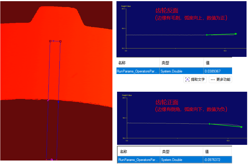
In lithium-ion battery production, protrusions or indentations at the edges of coated electrodes (thick edges or trailing edges) can affect battery performance and even cause short circuits. A line laser profile sensor installed downstream of the coating head scans the surface topography of the wet or dry film in real time and generates a two-dimensional profile curve. In conjunction with contour analysis tools within the software, the system calculates the average coating thickness, peak deviation, and edge slope, providing real-time feedback to the coating die for closed-loop control, thereby effectively improving yield rates. Additionally, the verticality of the tabs and the presence of any folding can be efficiently determined through contour scanning.
Scenario 3: Thread and Connector Inspection
For bolt threads, internal threads, or turned parts, the contour sensor scans around the axis once to reconstruct the complete 3D morphology of the thread. The algorithm automatically extracts parameters such as pitch, thread angle, and mean diameter, compares them with CAD standards, and determines whether they are out of tolerance. In connector pin inspection, the sensor can scan the height of an entire row of pins in a single pass, quickly detecting defects such as bent, shrunk, or misaligned pins, with efficiency far exceeding that of individual probe contact measurements.
Scenario 4: Flatness and Co-planarity Measurement
In PCB assembly inspection and chip placement inspection, the coplanarity of component surfaces directly affects soldering quality and the reliability of electrical connections. A line laser profilometer scans the entire placement area to capture the coordinates of the highest points on all solder balls, leads, or BGA solder balls. It then fits a reference plane using the least squares method and calculates the deviation of each point relative to the reference plane. Components exceeding the set threshold are automatically marked as defective, ensuring that subsequent processes are not affected.
Selection Guide:
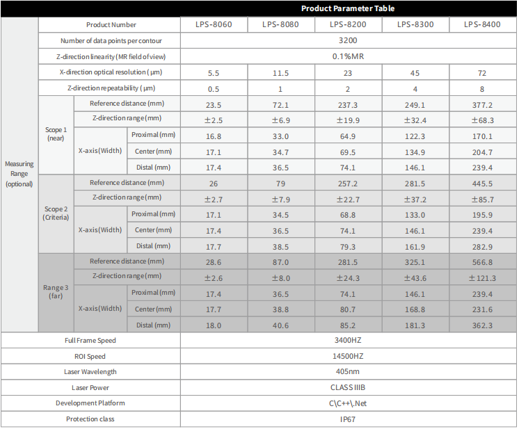
Different applications place varying emphasis on the requirements for profile sensors. Wide-field-of-view scanning (such as gap inspection on complete vehicles) requires models with a wide measurement range and low resolution; high-precision measurement (such as the height of solder balls on chips) requires models with a small field of view and high Z-axis repeatability. In addition, laser wavelength (blue light for highly reflective surfaces, red light for dark materials), the number of profile points (which affects detail resolution), and linearity (which determines measurement error) are technical specifications that must be comprehensively considered during selection.
Use Cases:

The line laser profile sensor is not a single-function product, but a flexible 3D inspection platform. Whether measuring height differences, flatness, step heights, angles, radii, or profile matching, it can perform automatic measurements with simple configuration. Deploying it on a production line is like equipping the quality control system with a pair of “eyes that can measure thickness,” leaving no room for height-related defects to hide.
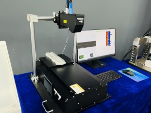
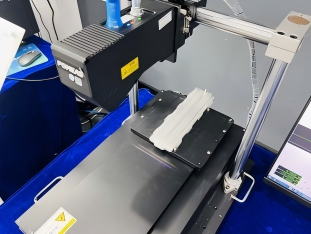
Product recommendation
TECHNICAL SOLUTION
MORE+You may also be interested in the following information
FREE CONSULTING SERVICE
Let’s help you to find the right solution for your project!

 ASK POMEAS
  PRICE INQUIRY
  REQUEST DEMO/TEST
  FREE TRIAL UNIT
  ACCURATE SELECTION
 - APPICATION CASE
- RESOURCE CENTER
- DOWNLOAD CENTER
SOLUTIONS SUPPORT
- ZOOM LENS SELECTION TOOL
- TELECENTRIC LENS SELECTION TOOL
- FA LENS SELECTION TOOL
- ZOOM RATIO TABLE
- CERTIFIED MODEL
SELECTION TOOL
- WHY POMEAS
- FAQ
- PRIVACY POLICY
- TERMS OF USE
- DELIVERY & RETURN POLICY
CUSTOMER CARE
 ADDRESS
Add.:No.68, Yongwei Road, Baizhoubian, Dongcheng District, Dongguan, China,523000
CONTACT
 Tel:+ 86-0769-2266 0867
 Fax:+ 86-0769-2266 0867
 E-mail:marketing@pomeas.com

Wechat QR code
Software Copyright :2021SR0176001 抄袭必究, 技术支持:誉新源科技