


I. Key Features of ZOOM LENSes

-
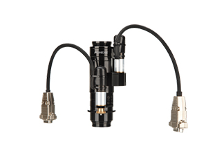
Continuously adjustable magnification; no need to change lenses or adjust mechanical structures – switch to a magnified field of view at the touch of a button;
-
Full-range magnification lock ensures the magnification remains stable and drift-free after zooming, with excellent control of image distortion;
-
Compatible with coaxial optical paths; can be used with ring or coaxial light sources, suitable for inspecting micro-wafers and chip pins;
-
Depth of field optimised for precision micro-components, ensuring consistently sharp imaging even for components with varying heights;
-
Integrated design compatible with automated equipment, supporting programme-controlled electronic zooming and suitable for assembly line inspection.
II. Mandatory Requirements for Semiconductor Testing Solutions

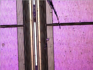
Semiconductor components vary enormously in size, ranging from entire wafers and packaged modules to micrometre-scale leads, solder balls and photolithographic patterns; a single-magnification lens cannot cater for all these requirements. There are several key requirements in the industry for inspection:
-
All-in-one solution: the same unit performs both macro-level full-surface screening and micro-level defect inspection, reducing changeover time associated with switching between multiple lenses;
-
Stable magnification accuracy ensures no drift in dimensional measurement data before and after zooming, guaranteeing the traceability of inspection results;
-
Compatible with automated production lines, supporting automatic programme-controlled magnification switching to match high-speed in-line inspection cycles;
-
High-fidelity imaging with low distortion and high resolution, accurately capturing minute defects such as scratches, cold solder joints, pinholes and chipped edges;
-
Compatible with confined installation spaces, featuring a compact optical path design suitable for equipment such as wafer inspection machines, AOI systems and probe stations.
III. Why is it generally said that ZOOM LENSes are more suitable for semiconductor inspection solutions?

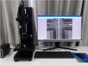
Semiconductor inspection requires both wide-area preliminary inspection and micron-level microscopic re-inspection; fixed-focus lenses can only provide a fixed field of view, and frequent lens changes slow down the production line and introduce repeat positioning errors.
ZOOM LENSes, with their core advantages of continuous electronically controlled zooming, stable magnification and the ability to cover multi-scale inspection with a single unit, perfectly meet the end-to-end inspection requirements for semiconductor wafers, chips and packaged components. Eliminating the need for multiple devices and frequent disassembly, assembly and calibration, they not only enhance production line inspection efficiency but also consistently ensure the accuracy of defect identification and dimensional verification, making them the mainstream choice for semiconductor vision inspection solutions.
Product recommendation
TECHNICAL SOLUTION
MORE+You may also be interested in the following information
FREE CONSULTING SERVICE
Let’s help you to find the right solution for your project!
 ASK POMEAS
  PRICE INQUIRY
  REQUEST DEMO/TEST
  FREE TRIAL UNIT
  ACCURATE SELECTION
- APPICATION CASE
- RESOURCE CENTER
- DOWNLOAD CENTER
SOLUTIONS SUPPORT
- ZOOM LENS SELECTION TOOL
- TELECENTRIC LENS SELECTION TOOL
- FA LENS SELECTION TOOL
- ZOOM RATIO TABLE
- CERTIFIED MODEL
SELECTION TOOL
- WHY POMEAS
- FAQ
- PRIVACY POLICY
- TERMS OF USE
- DELIVERY & RETURN POLICY
CUSTOMER CARE
 ADDRESS
Add.:No.68, Yongwei Road, Baizhoubian, Dongcheng District, Dongguan, China,523000
CONTACT
 Tel:+ 86-0769-2266 0867
 Fax:+ 86-0769-2266 0867
 E-mail:marketing@pomeas.com

Wechat QR code

Software Copyright :2021SR0176001 抄袭必究, 技术支持:誉新源科技