


In which fields can spectral autofocus microscopy systems be used?
Spectral autofocus microscopy systems are widely established as frontline tools in life sciences research, semiconductor wafer inspection, materials science characterisation and precision industrial quality control. In any scenario where microstructures need to be ‘seen clearly, measured accurately and tracked stably’, these systems play an irreplaceable role as ‘electronic eyes’.

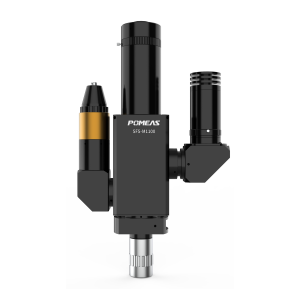
Why is ‘spectral’ added to ‘autofocus’?

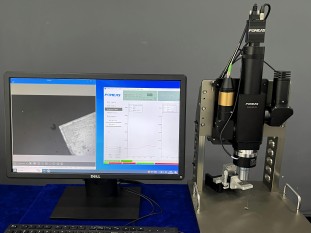
Traditional microscopes rely on mechanical stepping to locate the focal plane, which is slow and susceptible to interference from temperature and vibration. In contrast, spectral autofocus microscopy systems utilise broadband light or signals at specific wavelengths to analyse spectral changes at the focal plane in real time, achieving closed-loop locking within milliseconds. This means that even if the sample surface is uneven or thermal drift occurs during observation, the system can ‘adjust whilst viewing’, consistently producing the sharpest images, with the focal plane coordinates of every frame being traceable.
Four Key Application Areas
1. Life Sciences: ‘Time-lapse’ imaging of living cells and tissue sections

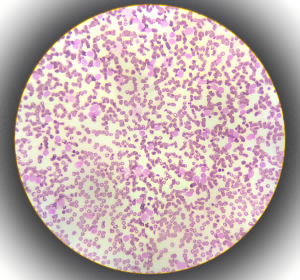
During prolonged live-cell imaging, cells adhere to the surface and move, whilst the liquid level of the culture medium also fluctuates slightly. Traditional focusing requires manual readjustment every few minutes, whereas the spectral autofocus system tracks the focal plane at a rate of several dozen times per second, enabling researchers to continuously record drug response processes for several hours, with every image remaining as sharp as the first. For thick tissue sections (such as brain slices), it can also combine spectral signals from different depths to automatically perform multi-layer focusing and stitching, helping pathologists to identify pathological areas more accurately.
2. Semiconductors and Microelectronics: A ‘Magic Mirror’ for Nanoscale Defects

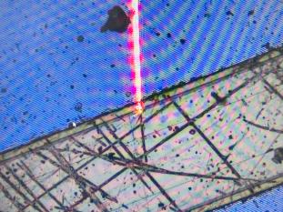
Due to the uneven thickness of the photoresist on the wafer surface and the extremely high aspect ratio of the trench structures, conventional reflective focusing systems are highly prone to ‘getting lost’. The spectral autofocus system utilises the interference characteristics of reflected spectra to precisely lock onto the optimal focal plane for different film layers. Even with a 10× objective, it can perform full-area automatic scanning of 200-millimetre wafers, enhancing the repeatability of defect detection to the nanometre level. From LED chips to MEMS sensors, this technology has become a standard component of yield control on production lines.
3. Materials Science: The ‘Surface Topographers’ of Two-Dimensional Materials and Coatings
Graphene, perovskite films, battery electrode coatings—the performance of these materials is highly dependent on surface topography and thickness uniformity. The spectral autofocus system can be used in conjunction with confocal or white-light interferometry modules to compensate in real time for sample tilt and warping during scanning. The high-precision 3D topography maps generated not only calculate surface roughness but also derive local refractive indices and absorption coefficients through spectral inversion, providing in situ data for the optimisation of new material formulations.
4. Industrial Quality Control and Precision Manufacturing: The Online ‘Gatekeeper’

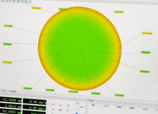
Fibre-optic end-face inspection, optical lens curvature measurement, precision mould microstructure comparison… Whilst production lines operate at high speed, the system performs loading, unloading, focusing, evaluation and sorting fully automatically. Single-point focusing time can be reduced to less than 20 milliseconds, and the system is insensitive to changes in ambient light; day-to-night transitions do not affect its repeatability.
Product recommendation
TECHNICAL SOLUTION
MORE+You may also be interested in the following information
FREE CONSULTING SERVICE
Let’s help you to find the right solution for your project!
 ASK POMEAS
  PRICE INQUIRY
  REQUEST DEMO/TEST
  FREE TRIAL UNIT
  ACCURATE SELECTION
- APPICATION CASE
- RESOURCE CENTER
- DOWNLOAD CENTER
SOLUTIONS SUPPORT
- ZOOM LENS SELECTION TOOL
- TELECENTRIC LENS SELECTION TOOL
- FA LENS SELECTION TOOL
- ZOOM RATIO TABLE
- CERTIFIED MODEL
SELECTION TOOL
- WHY POMEAS
- FAQ
- PRIVACY POLICY
- TERMS OF USE
- DELIVERY & RETURN POLICY
CUSTOMER CARE
 ADDRESS
Add.:No.68, Yongwei Road, Baizhoubian, Dongcheng District, Dongguan, China,523000
CONTACT
 Tel:+ 86-0769-2266 0867
 Fax:+ 86-0769-2266 0867
 E-mail:marketing@pomeas.com

Wechat QR code

Software Copyright :2021SR0176001 抄袭必究, 技术支持:誉新源科技