


4K Zoom Industry Lens Application On Semiconductor Inspection and Measuring Industry
COVID-19 has been attacked on the whole world in 2020, in the meantime, this year is the worst year of semiconductor industry affected by the Sino-US trade friction in recent years. Accordingly, it is also an opportunity for us.
From the view of national semiconductor production equipment market ( including Wafer Fab equipment +test&packaging equipment+accessory equipment, excluding crystalline silicon production equipment.), Our country China and South Korea has been leading the equipment investment in the year of 2020. The Foundry and storage semiconductor investments are hot on the market in China, which will push China to become the TOP1 of semiconductor equipment market scale for the first time. It can be seen that the country is actively advocating the development of domestic semiconductor industry.
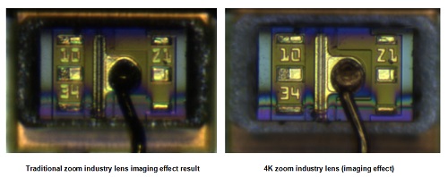
The upstream semiconductor production equipment industry has entered a golden period of development, and the scale of semiconductor testing equipment is expected to reach more than 100 billion in the future, which is both an opportunity and a challenge for the semiconductor vision detection and measurement industry. The industry has put more and more higher requirement on vision inspection and measuring. As the first lens of this type in China, POMEAS 4K zoom industry lens can significantly improve the detection capability in the application field of traditional zoom industrial lens and provide better solutions for the transformation and upgrading of related industries.
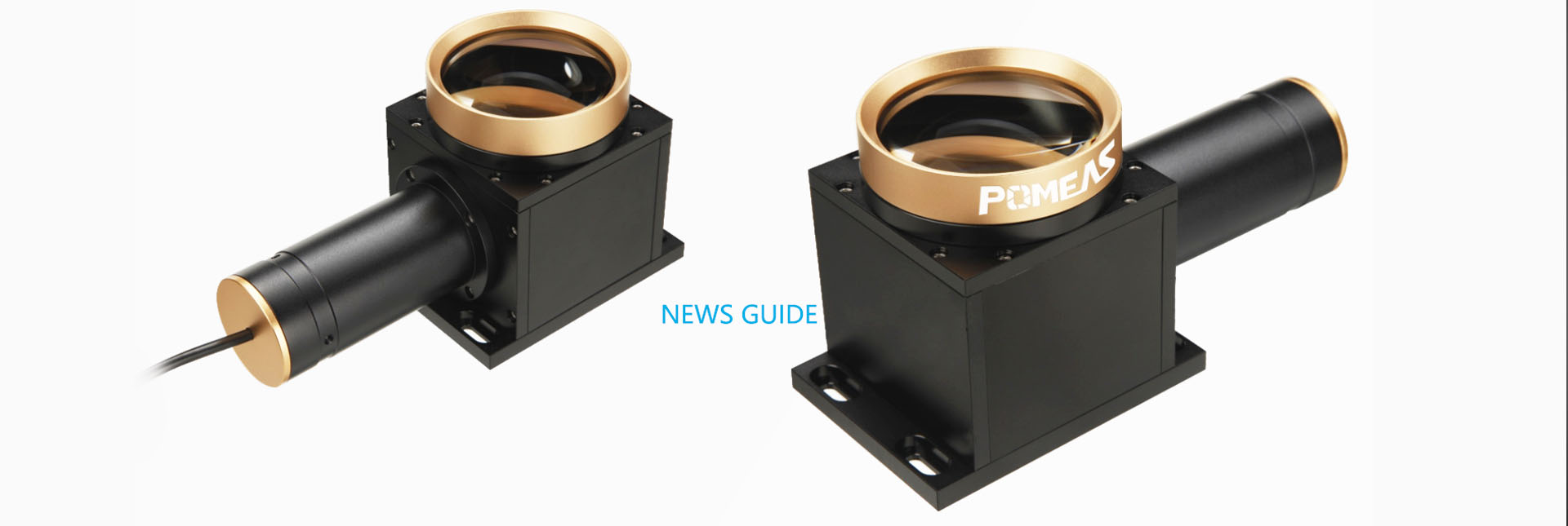
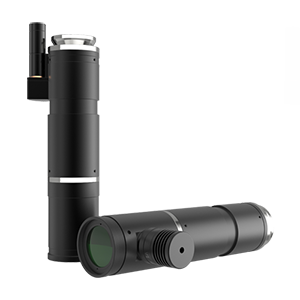
POMEAS 4K big FOV high-resolution zoom lens not only has excellent performance in continuously zooming, but also has big field of view and higher speed to capture larger view on imaging. It’s an ideal choice for high speed detection and accurate application. Compared with the traditional zoom system, the resolution of 4K zoom industrial lens is significantly improved at high magnification, the resolution of object square is increased from 3.95um to 2.8um, and the field of view is increased by more than 1.45X. At the same time, 4K HD zoom lens also adopts modular design. However, different from traditional zoom lens, this 4K zoom industrial lens has a variety of interface components, which can support a variety of camera interfaces. Match with different rear TV lens tubes, the maximum diagonal dimension to support camera target surface is up to 32mm.
Case 1: Semiconductor industry--Gold thread foot welding detection
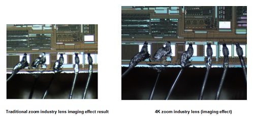
The 4K zoom industry lens has larger field of view, which can not only see all welding feet at one time, but also has a higher definition. It’s more beneficial to the identification of defect points.
Case 2: Semiconductor industry--thread breakage detection
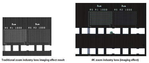
4k zoom industry lens provides clear imaging, high contrast and large field of vision, which is more convenient for accurate detection.
Case 3: Semiconductor industry--positioning detection
4K ultra HD zoom lens application in the field of image detection
At present, digital cameras with larger target surface and higher pixels are becoming the mainstream. The zoom lens used in traditional 2D image measurement is generally designed based on matching analog cameras. The disadvantages such as low resolution of the objective space, small imaging target surface and small field of vision have a great impact on the measurement accuracy and the convenience of use. Therefore, POMEAS launched 4k zoom industrial times, these problems can be effectively improved.
For more application case of 4k zoom lens, please continue to pay attention to the case center in POMEAS official website, we will continue to update.
Product recommendation
TECHNICAL SOLUTION
MORE+You may also be interested in the following information


FREE CONSULTING SERVICE
Let’s help you to find the right solution for your project!

 ASK POMEAS
  PRICE INQUIRY
  REQUEST DEMO/TEST
  FREE TRIAL UNIT
  ACCURATE SELECTION
 - APPICATION CASE
- RESOURCE CENTER
- DOWNLOAD CENTER
SOLUTIONS SUPPORT
- ZOOM LENS SELECTION TOOL
- TELECENTRIC LENS SELECTION TOOL
- FA LENS SELECTION TOOL
- ZOOM RATIO TABLE
- CERTIFIED MODEL
SELECTION TOOL
- WHY POMEAS
- FAQ
- PRIVACY POLICY
- TERMS OF USE
- DELIVERY & RETURN POLICY
CUSTOMER CARE
 ADDRESS
Add.:No.68, Yongwei Road, Baizhoubian, Dongcheng District, Dongguan, China,523000
CONTACT
 Tel:+ 86-0769-2266 0867
 Fax:+ 86-0769-2266 0867
 E-mail:marketing@pomeas.com

Wechat QR code
Software Copyright :2021SR0176001 抄袭必究, 技术支持:誉新源科技