


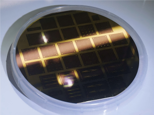
Spectral Confocal Sensors for Wafer Thickness Measurement Applications
Difficulties in measuring wafer thickness

1. Influence of wafer surface characteristics:
Surface roughness: the surface of the wafer may have a certain degree of roughness, which will lead to the scattering and reflection of light on the surface of the complexity of the situation, affecting the sensor on the reception and analysis of reflected light, thus reducing the accuracy of the measurement.
Material properties: different wafer materials on the absorption of light, reflection and refraction characteristics are different, for example, some special semiconductor materials may have a higher refractive index, which will make the light propagation path inside the wafer changes, affecting the results of thickness measurement.
2. The impact of the measurement environment:
Temperature changes: in the production and measurement of wafers in the process, temperature changes will lead to the size of the wafer a small expansion or contraction, thus affecting the accuracy of the thickness measurement. In addition, temperature changes may also affect the performance of the spectral confocal sensor, making its measurement results biased.
Vibration interference: vibration in the measurement environment will make the wafer and sensor relative displacement, resulting in unstable measurement results. Especially in industrial production sites, the operation of various mechanical equipment may produce vibration, the wafer thickness measurement interference.
3. The requirements of equipment accuracy:
Sensor resolution: With the continuous development of semiconductor processes, the thickness of the wafer is getting thinner and thinner, the resolution requirements of the measurement equipment is also getting higher and higher. Spectral confocal sensor needs to have a high enough resolution to accurately measure the wafer's small thickness changes.
Measurement range and linearity: The thickness range of a wafer can be large, and the sensor needs to maintain good linearity over the entire measurement range to ensure the accuracy of the measurement results. Otherwise, the measurement error may be different in different thickness ranges, affecting the accurate assessment of wafer thickness.
Advantages of Spectral Confocal Sensors for Wafer Thickness Measurement

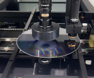
1. Non-contact measurement: it will not cause physical damage to wafers, avoiding scratches, pollution and other problems that may be caused by contact measurement, which is very important for high-precision wafer manufacturing.
2. High-precision measurement: capable of achieving nanometer resolution and micron-level measurement accuracy, which can meet the high-precision requirements of wafer thickness measurement.
3. Strong adaptability to transparent materials: for some transparent wafer materials, such as sapphire wafers, the spectral confocal sensor can accurately measure their thickness, while traditional measurement methods may be interfered by transparent materials.
4. Rapid measurement: the ability to quickly obtain the thickness information of the wafer, which improves the production efficiency and is suitable for on-line inspection in mass production.
5. Multi-parameter measurement: In addition to thickness measurement, the spectral confocal sensor can also simultaneously measure the wafer's surface topography, flatness and other parameters, providing more comprehensive information for wafer quality assessment.
Product recommendation
TECHNICAL SOLUTION
MORE+You may also be interested in the following information
FREE CONSULTING SERVICE
Let’s help you to find the right solution for your project!

 ASK POMEAS
  PRICE INQUIRY
  REQUEST DEMO/TEST
  FREE TRIAL UNIT
  ACCURATE SELECTION
 - APPICATION CASE
- RESOURCE CENTER
- DOWNLOAD CENTER
SOLUTIONS SUPPORT
- ZOOM LENS SELECTION TOOL
- TELECENTRIC LENS SELECTION TOOL
- FA LENS SELECTION TOOL
- ZOOM RATIO TABLE
- CERTIFIED MODEL
SELECTION TOOL
- WHY POMEAS
- FAQ
- PRIVACY POLICY
- TERMS OF USE
- DELIVERY & RETURN POLICY
CUSTOMER CARE
 ADDRESS
Add.:No.68, Yongwei Road, Baizhoubian, Dongcheng District, Dongguan, China,523000
CONTACT
 Tel:+ 86-0769-2266 0867
 Fax:+ 86-0769-2266 0867
 E-mail:marketing@pomeas.com

Wechat QR code
Software Copyright :2021SR0176001 抄袭必究, 技术支持:誉新源科技