


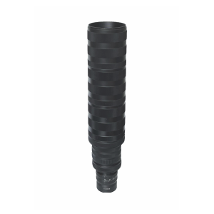
With the three core advantages of φ82mm large target surface, 0.22X-3.5X wide reference magnification, and vibration-proof optimized design, the 16K line scanning lens accurately covers the complex inspection needs of semiconductor, 3C electronics, printing, and other industries, redefining the Wide-format high-precision visual inspection standard.

1. φ82mm large target surface, wide-format inspection efficiency jumps up
The 16K line scanning lens adopts the industry-leading φ82mm target surface design, which can cover 1.2 meters wide at one time and reduce the need for multi-lens splicing. In the lithium battery wafer coating, PCB board defect detection and other scenarios, a single scanning can be completed in the entire surface imaging, efficiency increased by more than 50%. Combined with <0.05% ultra-low distortion technology, it ensures high consistency from the edge to the center of the image, providing an accurate data base for micron-level defect identification.
2. Full scene magnification coverage, flexible adaptation to multiple needs
The base magnification covers 0.22X-3.5X, supporting the whole process of inspection from macroscopic positioning to microscopic detail analysis. For example, in semiconductor wafer inspection, 0.22X magnification can scan the surface of 12-inch wafers in panoramic view, while 3.5X high-magnification local zoom can accurately identify scratches of 0.5 μm level; in the macro inspection of cell phone modules, 1.5X magnification combined with a line array camera realizes high-speed scanning of 1,000 frames per second, with a false positive detection rate of <0.001%.
3. Anti-vibration optimization, zero-shake imaging under high-speed movement
To address the problem of high-speed production line vibration, the lens is optimized with a conjugate distance of up to 2,182mm to ensure that the image is still stable at line speeds of 300mm/s or more. Combined with the optical anti-shaking algorithm and rigid structure, the MTF value is stabilized at more than 80lp/mm, which completely eliminates the influence of motion blur on the detection accuracy and is especially suitable for high-speed scenarios such as OLED evaporation, Mini LED solid crystal, and so on.
Application Scenarios
1. Semiconductor wafer defect detection: In the production of 12-inch wafers, 16K line scanning lens with 0.22X magnification Panoramic scanning of the wafer surface, combined with AI algorithms to accurately identify 0.5μm particle contamination and scratches, with a false detection rate of <0.001% and improved yields.
2. Mobile phone module macro inspection: for camera module lens set offset detection, 16K lines scanning lens with 1.5X magnification to achieve 800 lines per second high-speed scanning. Realize 800 lines per second high-speed scanning, with coaxial light source to accurately capture the lens offset (±5μm), the detection efficiency is 3 times higher than the traditional program, saving labor costs.
3. Analysis of color registration accuracy of printed products: In the wide-format printing production line, 16K line scanning lens with 0.35X magnification Covering a width of 1.5 meters, real-time detection of color register deviation (±0.05mm), combined with closed-loop control system to achieve color consistency increased by 40%.
Product recommendation
TECHNICAL SOLUTION
MORE+You may also be interested in the following information
FREE CONSULTING SERVICE
Let’s help you to find the right solution for your project!

 ASK POMEAS
  PRICE INQUIRY
  REQUEST DEMO/TEST
  FREE TRIAL UNIT
  ACCURATE SELECTION
 - APPICATION CASE
- RESOURCE CENTER
- DOWNLOAD CENTER
SOLUTIONS SUPPORT
- ZOOM LENS SELECTION TOOL
- TELECENTRIC LENS SELECTION TOOL
- FA LENS SELECTION TOOL
- ZOOM RATIO TABLE
- CERTIFIED MODEL
SELECTION TOOL
- WHY POMEAS
- FAQ
- PRIVACY POLICY
- TERMS OF USE
- DELIVERY & RETURN POLICY
CUSTOMER CARE
 ADDRESS
Add.:No.68, Chongwei Road, Baizhoubian, East district, Dongguan, China, 523000
CONTACT
 Tel:+ 86-0769-2266 0867
 Fax:+ 86-0769-2266 0867
 E-mail:marketing@pomeas.com

Wechat QR code
Software Copyright :2021SR0176001 抄袭必究, 技术支持:誉新源科技