


Applications of White Light Interferometric Profilometers in the Semiconductor Industry
In the semiconductor manufacturing industry, where the pursuit of extreme precision reigns supreme, nanoscale measurement of surface topography is pivotal to determining chip performance and yield rates. As technology nodes continue to shrink, traditional contact-based measurement methods can no longer meet the demands for non-destructive, high-accuracy, and high-efficiency inspection. As an advanced optical measurement technology, the white-light interferometric profilometer has become an indispensable precision measurement and quality control tool in the semiconductor industry, leveraging its unique advantages.

I. Introduction to the Working Principle of White Light Interferometric Profilometers

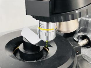
The white light interferometric profilometer is a non-contact three-dimensional surface topography measurement device based on the principle of white light interference. Its core workflow is as follows:
-
Interference occurs: The instrument splits a broad-spectrum white light beam into two paths. One beam illuminates the surface of the sample being measured, while the other beam strikes an internal reference mirror. After reflection, the two beams recombine, producing interference due to the optical path difference.
-
Signal Acquisition: A piezoelectric ceramic driver performs a precise vertical scan of the sample or interference objective. A detector (such as a CCD camera) records the signal representing the variation in interference light intensity across each pixel within the entire scan range as the scanning position changes.
-
Data Processing: The algorithm precisely calculates the position of the maximum interference fringe contrast from each pixel's interference signal, corresponding to the zero-path-difference point at that location. Ultimately, the height information from all pixels is synthesized to reconstruct a three-dimensional topography map of the sample surface.
This principle endows it with core capabilities such as nanometer-level vertical resolution, rapid scanning over large areas, and excellent adaptability to both diffuse and specular reflective surfaces.
II. Core Application Scenarios in the Semiconductor Industry
White light interferometry profilometers play a vital role in both front-end and back-end processes of semiconductor manufacturing:
-
Film Thickness and Uniformity Measurement: Used to measure the thickness of films formed by processes such as Chemical Vapor Deposition (CVD) and Physical Vapor Deposition (PVD), as well as their uniformity across the wafer, serving as a critical indicator for process monitoring.
-
CMP (Chemical Mechanical Polishing) Process Monitoring: Precisely measures the overall surface flatness and local step height of polished wafers to evaluate polishing effectiveness and prevent over- or under-polishing.
-
Photoresist Topography Analysis: Measures the 3D profile, sidewall angle, line width, and other parameters of photoresist patterns, providing direct data support for lithography process optimization.
-
Micro/Nano Structure Characterization: Precisely quantifies depth, width, and shape of three-dimensional microstructures such as MEMS devices, TSVs (Through-Silicon Vias), and microlens arrays.
-
Surface Roughness and Defect Detection: Evaluates surface roughness (parameters like Sa, Sq) of wafers, substrates, or polishing pads, and identifies microscopic defects such as scratches and particles.
III. Key Selection Criteria: Precision, Efficiency, and Stability
For the demanding semiconductor industry, selecting an appropriate white light interferometric profilometer requires key considerations:
-
Ultra-high precision and resolution: Must deliver sub-nanometer vertical resolution and nanometer repeatability to meet measurement demands of cutting-edge processes.
-
High-speed measurement and efficient throughput: Rapid scanning and data analysis capabilities, while maintaining accuracy, significantly enhance online or offline inspection efficiency to align with production cycle times.
-
Exceptional Environmental Immunity: Superior vibration suppression and temperature drift compensation mechanisms ensure stable, reliable data acquisition in both standard laboratories and near-production environments.
-
Robust Software Analysis Capabilities: The software must provide comprehensive analysis tools compliant with semiconductor industry standards (e.g., step height, roughness, volume, area) and generate reports adhering to quality management specifications.
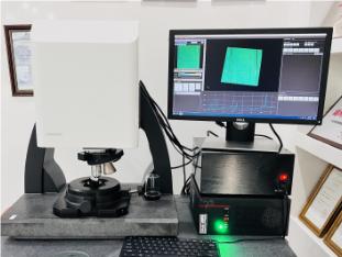
IV. Professional Solutions: POMEAS WLI1000 Series
Facing these stringent requirements, seasoned industry manufacturers have delivered mature and reliable solutions. Take the WLI1000 series white light interferometric profilometer from POMEAS Optics as an example. Designed specifically for surface metrology in precision manufacturing, its features align closely with the demands of the semiconductor industry.
Employing a stable white light interferometry system and high-precision piezoelectric scanning technology, it achieves nanometer-level measurement accuracy. Its design emphasizes measurement repeatability and long-term stability. Even in environments with slight vibrations, optimized algorithms ensure reliable results, making it suitable not only for metrology labs but also for deployment in near-process quality control. Furthermore, its efficient scanning speed and intuitive, professional analysis software significantly enhance workflow efficiency from measurement to data analysis, helping process engineers quickly identify issues and optimize parameters.
Product recommendation
TECHNICAL SOLUTION
MORE+You may also be interested in the following information
FREE CONSULTING SERVICE
Let’s help you to find the right solution for your project!

 ASK POMEAS
  PRICE INQUIRY
  REQUEST DEMO/TEST
  FREE TRIAL UNIT
  ACCURATE SELECTION
 - APPICATION CASE
- RESOURCE CENTER
- DOWNLOAD CENTER
SOLUTIONS SUPPORT
- ZOOM LENS SELECTION TOOL
- TELECENTRIC LENS SELECTION TOOL
- FA LENS SELECTION TOOL
- ZOOM RATIO TABLE
- CERTIFIED MODEL
SELECTION TOOL
- WHY POMEAS
- FAQ
- PRIVACY POLICY
- TERMS OF USE
- DELIVERY & RETURN POLICY
CUSTOMER CARE
 ADDRESS
Add.:No.68, Chongwei Road, Baizhoubian, East district, Dongguan, China, 523000
CONTACT
 Tel:+ 86-0769-2266 0867
 Fax:+ 86-0769-2266 0867
 E-mail:marketing@pomeas.com

Wechat QR code
Software Copyright :2021SR0176001 抄袭必究, 技术支持:誉新源科技