


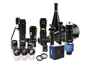
What are some successful applications of wafer inspection lenses?
Wafer inspection lenses are widely used in the semiconductor industry for applications such as detecting surface defects on wafers, measuring microscopic patterns and structures, and performing quality inspections during the lithography process. High-resolution microscope lenses or specialized industrial camera lenses are commonly used in conjunction with inspection equipment. The following section discusses lens selection based on real-world scenarios.

Case Study 1: Surface Scratches and Particle Detection

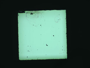
On a 12-inch wafer production line, false positives for surface scratches and edge chipping were previously high due to perspective distortion caused by standard lenses. After adopting a dual-telecentric lens system, combined with coaxial illumination and a 20-megapixel industrial camera, the parallel optical path eliminated perspective distortion, resulting in approximately a threefold increase in scratch contrast. Production line data shows that the detection rate reached 99.7%, false positives were reduced by approximately 80%, and the inspection time per wafer was approximately 9 seconds. The dual-telecentric structure minimizes distortion, ensuring consistent imaging at both the center and edges, making it suitable for detecting micron-level scratches and particulate contaminants.
Case Study 2: Detection of Microcracks in Edge Chamfers

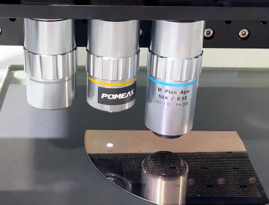
The cracks at the chamfered edges are very fine and difficult to see under bright-field illumination. The actual solution employs a 2x to 6x telecentric lens paired with collimated blue LED illumination to capture scattered light in dark-field mode. Due to the short wavelength of blue light and its small diffraction limit, combined with the camera’s quantum efficiency, the single-pixel resolution can reach 0.58 micrometers, enabling the stable detection of microcracks in chamfers as small as 1.8 micrometers. This combination balances speed and sensitivity.
Case Study 3: Detection of Internal Cracks in Silicon Wafers
Silicon is opaque to visible light but transparent to short-wave infrared radiation. For subsurface defects such as internal bubbles and microcracks, a short-wave infrared lens is used with a light source covering the 400 nm to 1,700 nm wavelength range to capture images via backside transmission. Scattering is enhanced at defect locations, forming dark streaks or dark spots that are captured by an infrared scanner. This approach has already been applied in cutting line inspection and the identification of bonding interface features.
Case Study 4: Measurement of Lithographic Patterns and Structures
Inspection of pattern integrity and line width measurement after lithography require a balance between resolution and field of view. A particular inspection solution employs a wide-spectrum, wide-field-of-view microscope objective with an operating wavelength range of 420 nm to 1,064 nm, a magnification of 10x, a visible light resolution of 0.88 micrometers, a near-infrared resolution of 1.35 micrometers, and a field of view of 3.3 mm. Compared to the approximately 2.65 mm objective field of view typical of common commercial microscope objectives, this provides a larger single-image field of view, thereby improving inspection efficiency. The apochromatic design ensures imaging quality across the entire spectral range.
Case Study 5: Multi-Level Detection
ZOOM LENS solutions cover a range from 0.05x to 0.5x, enabling switching between full-area scanning and localized enhanced inspection at a single workstation, and meeting multi-level requirements ranging from overall wafer appearance to chip structural dimensions.
From the surface to the interior, and from the edges to the patterns, the selection of wafer inspection lenses centers on defect visibility and inspection cycle time. High-resolution microscopic lenses, dual-telecentric lenses, short-wave infrared lenses, and broad-spectrum objectives are common and effective choices.
Product recommendation
TECHNICAL SOLUTION
MORE+You may also be interested in the following information
FREE CONSULTING SERVICE
Let’s help you to find the right solution for your project!
 ASK POMEAS
  PRICE INQUIRY
  REQUEST DEMO/TEST
  FREE TRIAL UNIT
  ACCURATE SELECTION
- APPICATION CASE
- RESOURCE CENTER
- DOWNLOAD CENTER
SOLUTIONS SUPPORT
- ZOOM LENS SELECTION TOOL
- TELECENTRIC LENS SELECTION TOOL
- FA LENS SELECTION TOOL
- ZOOM RATIO TABLE
- CERTIFIED MODEL
SELECTION TOOL
- WHY POMEAS
- FAQ
- PRIVACY POLICY
- TERMS OF USE
- DELIVERY & RETURN POLICY
CUSTOMER CARE
 ADDRESS
Add.:No.68, Yongwei Road, Baizhoubian, Dongcheng District, Dongguan, China,523000
CONTACT
 Tel:+ 86-0769-2266 0867
 Fax:+ 86-0769-2266 0867
 E-mail:marketing@pomeas.com

Wechat QR code

Software Copyright :2021SR0176001 抄袭必究, 技术支持:誉新源科技