


I. Background of the Proposal

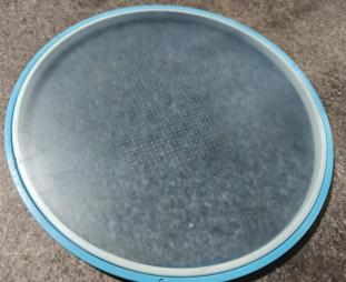
The test objects are small—micro IC/LED chips measuring 0.5 × 0.2 mm, bare die with an area of approximately 0.1 mm², or ultra-small packaged devices—commonly used in products such as cell phones, TWS earbuds, smartwatches/fitness trackers, tablets/laptops, Mini LED backlit TVs/monitors, automotive instrument clusters/ambient lighting, medical wearables, IoT modules, and micro-sensors.
II. Testing Requirements

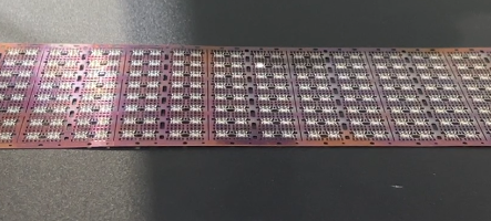
(1) Requirement: Visual quality inspection of micro IC/LED chips
(2) Challenge: Fixed-magnification microscopes either show only the entire chip—making it difficult to see the bond wires—or, when magnified to view the bond wires, fail to quickly locate the chip. The customer needs a single optical system capable of low-magnification panoramic positioning and high-magnification inspection of bond wires, electrodes, chipped edges, and contaminants;
III. Solutions

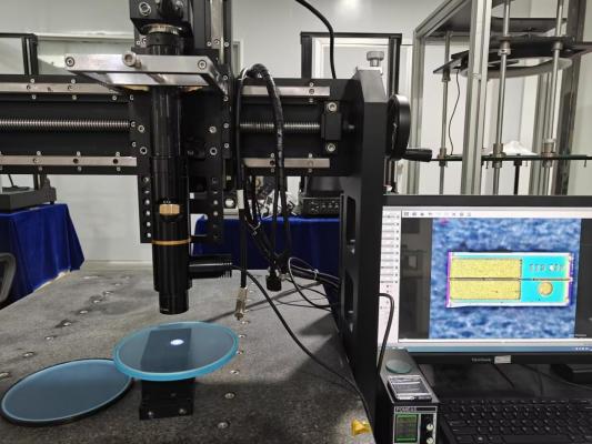
(1) Solution: Use a 0.55–7.6X continuously variable industrial lens (14X ZOOM LENS) paired with a 5-megapixel color smart microscope camera
(2) Architecture Analysis:
① The entire system features a 0.55–7.6X continuously variable industrial objective (14X ZOOM LENS) as its core imaging unit. Equipped with a 5-megapixel color smart microscope camera and coaxial illumination using high-brightness LED bulbs, and combined with a precision height-adjustable stand and an XY-axis stage, it forms an integrated microscopic observation solution that combines “low-magnification panoramic positioning” with “high-magnification detail observation”;
② The coaxial design of the lens and camera allows for continuous switching from wide-field views to micron-level details without changing objectives during the zoom process. The uniformity of the coaxial illumination has been specifically optimized to prevent overexposure and vignetting on highly reflective chip surfaces;
③ Images can be simultaneously output to a monitor or inspection software, facilitating simultaneous observation and archiving by multiple users.
IV. Features of the Plan
1. The microscope system is equipped with a camera that utilizes the latest color correction algorithms, delivering high image clarity and color accuracy, as well as fine image detail;
2. Lens features: Ultra-high zoom ratio and excellent optical performance; at low magnifications, it provides a wider field of view, while at high magnifications, it offers higher resolution; it features a built-in high-brightness, large-diameter LED with coaxial illumination, ensuring excellent uniformity.
V. How the System Works:

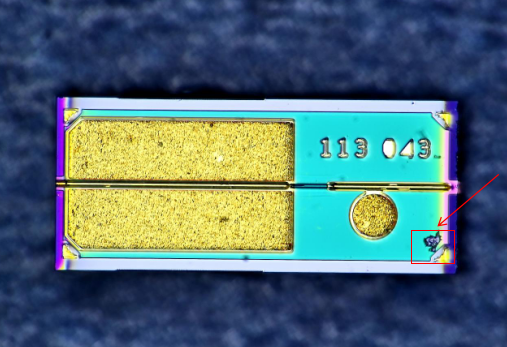
1. First, use the low-magnification end (0.55X) to quickly capture a panoramic image of the entire chip or the entire tray of devices, locate the target, and resolve the issue of “unable to find the chip” under high-magnification fields of view;
2. Smoothly switch to the desired magnification (up to 7.6X) by rotating the zoom ring; while keeping the focus and the center of the field of view essentially unchanged, sequentially inspect defect areas such as wire bonds, electrodes, chipped edges, and contamination;
3. Utilize the high-resolution imaging and color correction algorithms of the 5-megapixel color camera to measure defect dimensions and save images, outputting high-definition image data that can be used for defect determination and traceability.
VI. Conclusion

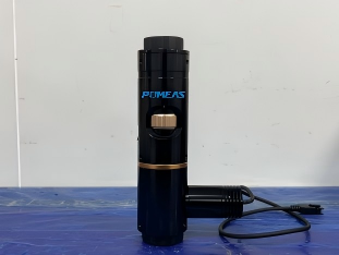
1. By pairing a 0.55X–7.6X continuously variable ZOOM LENS with a 500W color smart microscope camera, this system simultaneously achieves “low-magnification panoramic positioning” and “high-magnification detailed observation” within a single optical system, thereby resolving the long-standing issue of fixed-magnification microscopes being unable to balance field of view and resolution in a single solution;
2. The lens features built-in high-brightness, large-bead coaxial illumination with excellent uniformity. Combined with the camera’s latest color correction algorithm, defects such as chipped edges, contamination, and abnormal bonding lines on chip surfaces are clearly visible. Both image detail and color accuracy meet the requirements for visual inspection and evidence collection on packaging and testing production lines;
3. The entire system features a compact design, and the zoom process requires no objective lens changes. A single operator can complete the entire workflow—from positioning to evaluation—making it suitable for deployment in scenarios such as semiconductor packaging, incoming material inspection, shipment sampling, and failure analysis.
Product recommendation
TECHNICAL SOLUTION
MORE+You may also be interested in the following information
FREE CONSULTING SERVICE
Let’s help you to find the right solution for your project!
 ASK POMEAS
  PRICE INQUIRY
  REQUEST DEMO/TEST
  FREE TRIAL UNIT
  ACCURATE SELECTION
- APPICATION CASE
- RESOURCE CENTER
- DOWNLOAD CENTER
SOLUTIONS SUPPORT
- ZOOM LENS SELECTION TOOL
- TELECENTRIC LENS SELECTION TOOL
- FA LENS SELECTION TOOL
- ZOOM RATIO TABLE
- CERTIFIED MODEL
SELECTION TOOL
- WHY POMEAS
- FAQ
- PRIVACY POLICY
- TERMS OF USE
- DELIVERY & RETURN POLICY
CUSTOMER CARE
 ADDRESS
Add.:No.68, Yongwei Road, Baizhoubian, Dongcheng District, Dongguan, China,523000
CONTACT
 Tel:+ 86-0769-2266 0867
 Fax:+ 86-0769-2266 0867
 E-mail:marketing@pomeas.com

Wechat QR code

Software Copyright :2021SR0176001 抄袭必究, 技术支持:誉新源科技