


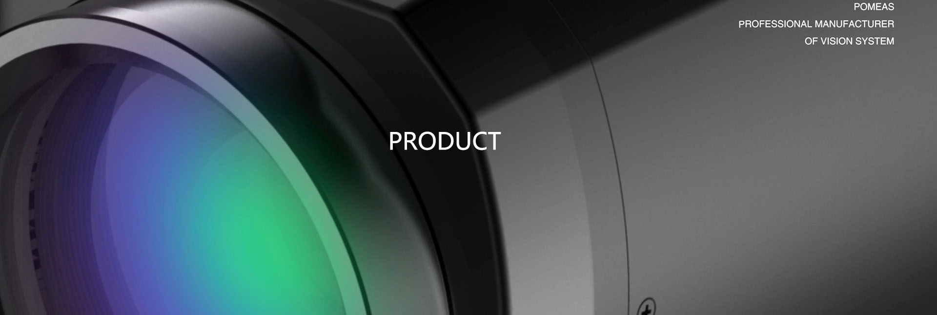
Industrial vision lighting refers to lighting equipment used in machine vision systems, designed to provide stable, uniform, and controllable illumination for visual inspection, thereby improving image quality and inspection accuracy. It does more than simply “illuminate objects”; it uses techniques such as bright-field, dark-field, coaxial, backlighting, and line scanning to reveal particles, scratches, pattern boundaries, and variations in the adhesive layer on the wafer surface. Taking wafer inspection as an example, the light source must often be matched to the lens, and different inspection stages require different lenses.

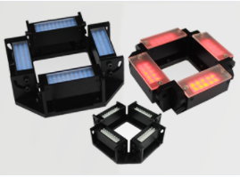
Particle and Scratch Detection: Dark-field Compound Microscope Objective Lens

In a case study involving the inspection of particles and scratches on a wafer surface—where the sample surface is highly reflective and the defects are minute—the system employs dark-field illumination in conjunction with a long-working-distance objective lens. The dark-field illumination creates a dark background against the smooth surface, while particles and scratches produce scattered light; the objective lens captures micrometer-level details. If a standard fixed-focus lens were used, it would not provide sufficient resolution; if the working distance were too short, it would be prone to interference with the wafer surface.
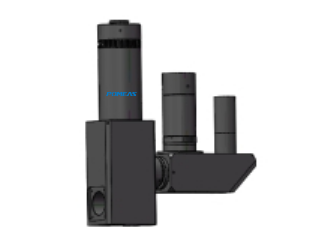
Alignment and Dimension Measurement: Dual-telephoto Lenses with Coaxial or Backlighting

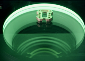
In wafer alignment and critical dimension measurement applications, a common approach involves using a pair of telecentric lenses in conjunction with coaxial or backlighting. Telecentric lenses minimize magnification errors caused by variations in the object-to-lens distance, making them suitable for measuring pattern positions, apertures, and edges. Backlighting is used to highlight contours, while coaxial lighting is used to identify surface markings. These applications focus more on geometric consistency than on resolution alone.
Full-Frame Scanning: Line-scan camera with a line light source
Line-scan lenses are commonly used in applications involving the scanning of an entire wafer surface. When paired with a line light source for line-by-line imaging, they are well-suited for uniform scanning of large areas, balancing both image width and efficiency. The uniformity of the line light source directly affects the consistency of the scanned image, and the lens must be compatible with the line-scan camera.
Special Response Detection: UV Lens with UV Light Source
In applications involving photoresist, fluorescence, or UV-responsive detection, specialized UV lenses and UV light sources are used. These solutions take advantage of differences in how materials respond to specific wavelength bands to observe features that are not visible under ordinary visible light. The lenses must provide good transmittance and imaging quality in that wavelength band.
Wide-Field Visual Inspection: Fixed-Focus Lens with Ring Light or Strip Light
Some wafer appearance inspection applications also use large-aperture, high-resolution fixed-focus lenses, in combination with annular or strip lighting, to inspect for chipped edges, contamination, and packaging areas within a wide field of view. Their advantages include a flexible field of view and relatively simple system integration; however, they are typically superseded by microscope objectives or telecentric lenses when inspecting for fine defects.
Product recommendation
TECHNICAL SOLUTION
MORE+You may also be interested in the following information
FREE CONSULTING SERVICE
Let’s help you to find the right solution for your project!
 ASK POMEAS
 PRICE INQUIRY
 REQUEST DEMO/TEST
 FREE TRIAL UNIT
 ACCURATE SELECTION

- APPICATION CASE
- RESOURCE CENTER
- DOWNLOAD CENTER
SOLUTIONS SUPPORT
- ZOOM LENS SELECTION TOOL
- TELECENTRIC LENS SELECTION TOOL
- FA LENS SELECTION TOOL
- ZOOM RATIO TABLE
- CERTIFIED MODEL
SELECTION TOOL
- WHY POMEAS
- FAQ
- PRIVACY POLICY
- TERMS OF USE
- DELIVERY & RETURN POLICY
CUSTOMER CARE
 ADDRESS
Add.:No.68, Yongwei Road, Baizhoubian, Dongcheng District, Dongguan, China,523000
CONTACT
 Tel:+ 86-0769-2266 0867
 Fax:+ 86-0769-2266 0867
 E-mail:marketing@pomeas.com

Wechat QR code

Software Copyright :2021SR0176001 抄袭必究, 技术支持:誉新源科技