


Is there a difference between co-planarity testing and flatness testing?
In the precision manufacturing, semiconductor, and electronics assembly industries, coplanarity is a key metric that affects assembly yield and solder joint reliability, and coplanarity inspection is also a critical component of quality control on production lines. Many manufacturing professionals are unclear about the definition of coplanarity inspection, its applicable scenarios, and appropriate inspection methods. This article addresses these core issues.

I. What Is Common Surface Detection?

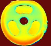
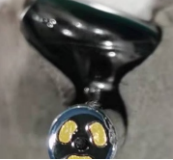
Coplanarity, simply put, is a geometric parameter that indicates whether multiple features—such as land marks, terminals, solder balls, or pins—lie on the same reference plane. Coplanarity inspection involves measuring the height difference between the highest and lowest points of these features to determine whether they fall within the tolerance range.
Poor coplanarity can lead to many production risks: uneven pin heights and lifted solder balls can cause cold solder joints, poor contact, and excessive assembly gaps, making the product prone to issues such as signal instability and functional failure during subsequent use. Unlike conventional flatness inspection, coplanarity inspection targets multiple discrete points rather than a continuous, complete plane, which is also what makes it challenging to inspect. Traditional manual inspection and simple jig-based methods suffer from poor stability and low efficiency; consequently, non-contact optical inspection has become the mainstream approach today.
II. Which Products Require Coplanarity Testing?

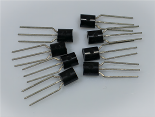
Coplanarity inspection focuses on high-density, precision-assembled products, particularly components with strict requirements for soldering and contact alignment. Semiconductor packaging products are the most common inspection targets, including chips in BGA, LGA, QFP, and PGA packages; the coplanarity of the solder balls and leads on the chip’s underside directly determines the yield rate of SMT placement and soldering. Various connector terminals, pin headers, and FPC connector pins also require inspection, as fine pins are prone to warping, lifting, or shrinking, which can lead to contact failure.
In addition, certain consumer electronics and automotive electronic components—such as module contacts, spring contacts, and conductive contacts—as well as some precision structural parts, including multi-contact metal spring assemblies and micro-metal contact components, all require coplanarity control. These products feature minute contact points with micron-level tolerance requirements; if coplanarity exceeds specifications, the cost of rework for entire batches can be extremely high.
III. Which Methods Are Suitable for Coplanarity Testing?

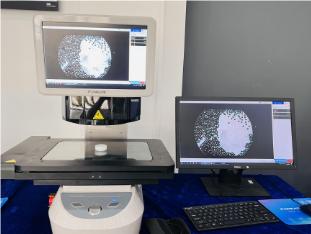
The core of coplanarity inspection is the acquisition of 3D height data. 2D vision can only capture planar contours and cannot obtain height information; therefore, it is generally not suitable for standalone coplanarity assessment. Mainstream solutions primarily rely on 3D optical inspection, with different solutions suited for varying levels of accuracy, speed, and material scenarios.
1. Line laser profile inspection solution: This method uses laser triangulation to capture contour heights. It is suitable for high-speed, in-line inspection on production lines and is well-suited for linearly arranged pins, such as those found in connectors and pin headers. It offers moderate cost-effectiveness, is stable and reliable for most metal pins, and is suitable for 100% inspection on high-volume assembly lines.
2. Structured light 3D vision solutions reconstruct the three-dimensional topography of workpieces by projecting encoded stripes. They are suitable for simultaneous multi-point acquisition across a surface, capturing the heights of all points on an entire surface in a single image. These solutions are well-suited for array-distributed solder balls, such as those found in BGAs and LGAs, offering high inspection efficiency and making them ideal for offline or in-line spot checks during the packaging stage.
3. Spectral confocal inspection solutions offer higher precision, reaching the micrometer or even submicrometer level. They can reliably capture data from reflective, curved, and minute solder balls, making them suitable for chips and micro-contacts requiring ultra-high precision. Their drawbacks include a relatively small field of view and slower speed; they are primarily used for laboratory sampling and quality verification of high-end precision components.
4. Contact-type probe measurement solutions offer stable accuracy; however, because they involve physical contact, they are prone to scratching tiny solder balls and soft leads. They are also slow and are generally used only for laboratory sampling and verification; they are not suitable for high-volume online inspection on production lines.
Co-plane inspection is a critical process for controlling the quality of multi-contact assemblies; the primary items inspected include chip packages, connector terminals, and various types of precision conductive contacts.

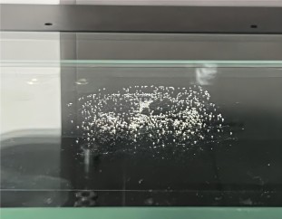
When selecting a system, you can categorize options based on specific requirements: for high-volume online production, prioritize line lasers; for array solder balls requiring multi-point simultaneous measurement, prioritize structured light; and for ultra-high-precision micro-inspection, choose a spectral confocal solution. Selecting the appropriate inspection solution can effectively reduce defects such as cold solder joints and poor contact, thereby stabilizing the finished product yield.
Product recommendation
TECHNICAL SOLUTION
MORE+You may also be interested in the following information
FREE CONSULTING SERVICE
Let’s help you to find the right solution for your project!

 ASK POMEAS
 PRICE INQUIRY
 REQUEST DEMO/TEST
 FREE TRIAL UNIT
 ACCURATE SELECTION

- APPICATION CASE
- RESOURCE CENTER
- DOWNLOAD CENTER
SOLUTIONS SUPPORT
- ZOOM LENS SELECTION TOOL
- TELECENTRIC LENS SELECTION TOOL
- FA LENS SELECTION TOOL
- ZOOM RATIO TABLE
- CERTIFIED MODEL
SELECTION TOOL
- WHY POMEAS
- FAQ
- PRIVACY POLICY
- TERMS OF USE
- DELIVERY & RETURN POLICY
CUSTOMER CARE
 ADDRESS
Add.:No.68, Yongwei Road, Baizhoubian, Dongcheng District, Dongguan, China,523000
CONTACT
 Tel:+ 86-0769-2266 0867
 Fax:+ 86-0769-2266 0867
 E-mail:marketing@pomeas.com

Wechat QR code

Software Copyright :2021SR0176001 抄袭必究, 技术支持:誉新源科技