


I. Key Advantages of the 12.5x ZOOM LENS

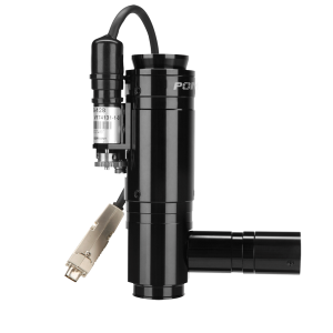
1. High Resolution and Low Distortion
With a resolution of up to 500 line pairs per millimeter and a distortion rate of less than 0.1%, it clearly displays key parameters such as the width and spacing of transistor gate lines. For example, when inspecting 7nm process wafers, traditional lenses produce blurry images at high magnifications, making it difficult to distinguish subtle line distortions. In contrast, the 12.5x lens can accurately capture nanoscale defects, preventing chip performance issues caused by missed defects.
2. High Zoom Ratio and Flexible Field of View
With a zoom range of 0.58x–7.5x and a field of view spanning 1.47–18.3 mm (based on a 2/3-inch camera), it simultaneously meets the demands of both macro scanning and micro-level observation. For instance, in transistor inspection, low magnification allows for rapid localization of chip areas across the entire wafer, while high magnification focuses on the gate structure of individual transistors, enabling efficient “one-click switching” inspection.
3. Mechanical Compensation and Image Plane Stabilization Technology
Through cam curve design, image plane displacement during zoom is controlled within ±0.02 mm, ensuring image stability. This feature is particularly critical in automated production lines, as it prevents image blurring caused by mechanical vibration or frequent zooming, thereby improving inspection repeatability to ±5 μm.
II. Typical Applications in Transistor Testing

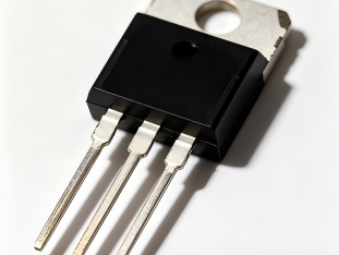
1. Gate Structure Inspection
In 7nm and smaller processes, transistor gate line widths may be less than 10nm, making them difficult to inspect with traditional lenses due to insufficient resolution. The 12.5x lens, featuring a high numerical aperture (N.A. > 0.3) design and paired with a coaxial light source, can clearly reveal subtle defects at the gate edges, such as line distortion and width anomalies.
2. Multi-layer Interconnect Structure Inspection
The multi-layer metal interconnects in transistors require a lens with a large depth of field. By optimizing the aperture and the spacing between lens groups, the 12.5x lens maintains a 5mm depth of field even at high magnification, enabling clear imaging of metal layers at different heights simultaneously and preventing missed defects caused by insufficient depth of field.
3. High-Density Solder Joint Inspection
In BGA-packaged chips, the spacing between transistor pin solder joints may be less than 0.3 mm. With an ultra-short working distance of 77.8 mm, the 12.5x lens can focus closely on the surface of solder joints to detect defects such as cold solder joints and incomplete soldering. When combined with an annular light source, it enhances surface texture contrast, improving inspection accuracy.
III. Recommendations for Selection and Implementation

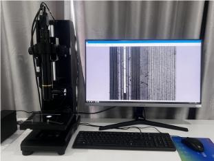
1. Coordinated Light Source Design
Select coaxial lighting, ring lighting, or backlighting based on the inspection scenario.
2. Support for Software Customization
Choose a lens manufacturer that provides an SDK, supporting multi-language programming to facilitate integration with automated inspection systems.
3. Environmental Adaptability Considerations
In semiconductor manufacturing environments, attention must be paid to the lens’s shock resistance, dust resistance, and temperature adaptability. The 12.5x lens features an all-metal body and IP67-rated protection, enabling stable operation in environments with intense vibration and high dust levels, thereby meeting the stringent requirements of production lines.
Product recommendation
TECHNICAL SOLUTION
MORE+You may also be interested in the following information
FREE CONSULTING SERVICE
Let’s help you to find the right solution for your project!

 ASK POMEAS
  PRICE INQUIRY
  REQUEST DEMO/TEST
  FREE TRIAL UNIT
  ACCURATE SELECTION
- APPICATION CASE
- RESOURCE CENTER
- DOWNLOAD CENTER
SOLUTIONS SUPPORT
- ZOOM LENS SELECTION TOOL
- TELECENTRIC LENS SELECTION TOOL
- FA LENS SELECTION TOOL
- ZOOM RATIO TABLE
- CERTIFIED MODEL
SELECTION TOOL
- WHY POMEAS
- FAQ
- PRIVACY POLICY
- TERMS OF USE
- DELIVERY & RETURN POLICY
CUSTOMER CARE
 ADDRESS
Add.:No.68, Yongwei Road, Baizhoubian, Dongcheng District, Dongguan, China,523000
CONTACT
 Tel:+ 86-0769-2266 0867
 Fax:+ 86-0769-2266 0867
 E-mail:marketing@pomeas.com

Wechat QR code

Software Copyright :2021SR0176001 抄袭必究, 技术支持:誉新源科技