


What is a high-precision autofocus tool microscope?

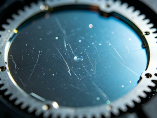
In fields such as industrial inspection and scientific research, detecting microscopic defects and observing microstructures requires precise and efficient tools, making high-precision autofocus tool microscopes the go-to choice. Equipped with an intelligent autofocus system, these microscopes eliminate the need for repeated manual focusing, quickly and accurately locking onto the focal point. This overcomes the limitations of traditional manual focusing, making microscopic observation more efficient and precise.
High-precision autofocus tool microscopes are an upgraded version of traditional microscopes. Their core advantage lies in their intelligent autofocus capability, which quickly adjusts the distance between the objective lens and the sample to maintain image clarity. These microscopes are suitable for a wide range of applications, including the inspection of precision industrial components, semiconductor wafer screening, and scientific material analysis, effectively addressing many of the shortcomings of traditional microscopes.
Features of the High-Precision Autofocus Tool Microscope

Traditional microscopes rely on manual focusing, which is time-consuming and labor-intensive, and is prone to out-of-focus images and missed observations. This results in low efficiency and inconsistent results during batch testing. In contrast, high-precision autofocus models utilize intelligent algorithms and precision sensor technology to standardize and automate the observation process, thereby lowering the learning curve and significantly improving testing accuracy.
Advantages of the POMEAS MICRO IMAGE3 Digital Microscope System

The POMEAS MICRO IMAGE3 digital microscopy system is the industry’s first infrared non-destructive wafer-penetrating AOI microscope to utilize laser focusing. Combining observation, imaging, and measurement into a single system, it offers outstanding advantages: it features high-definition resolution surpassing that of the naked eye, and when paired with Z-Stack rapid imaging technology, it can capture clear, fully focused images of complex samples with a single click; Operation is intuitive, allowing for 2D and 3D measurements with just a mouse, thereby eliminating human error; the laser focusing system responds in milliseconds, and when combined with infrared non-destructive technology, it can penetrate wafers to observe inner layers without damaging the sample; it supports seamless zoom from 20X to 8000X, paired with 4K resolution, to meet the demands of multiple application scenarios.
Applications of the MICRO IMAGE3 Digital Microscope System
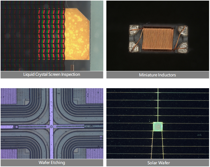
It is widely used in semiconductor wafer inspection, chip packaging, material surface analysis, and quality control of precision components.
Product recommendation
TECHNICAL SOLUTION
MORE+You may also be interested in the following information
FREE CONSULTING SERVICE
Let’s help you to find the right solution for your project!
 ASK POMEAS
  PRICE INQUIRY
  REQUEST DEMO/TEST
  FREE TRIAL UNIT
  ACCURATE SELECTION
- APPICATION CASE
- RESOURCE CENTER
- DOWNLOAD CENTER
SOLUTIONS SUPPORT
- ZOOM LENS SELECTION TOOL
- TELECENTRIC LENS SELECTION TOOL
- FA LENS SELECTION TOOL
- ZOOM RATIO TABLE
- CERTIFIED MODEL
SELECTION TOOL
- WHY POMEAS
- FAQ
- PRIVACY POLICY
- TERMS OF USE
- DELIVERY & RETURN POLICY
CUSTOMER CARE
 ADDRESS
Add.:No.68, Yongwei Road, Baizhoubian, Dongcheng District, Dongguan, China,523000
CONTACT
 Tel:+ 86-0769-2266 0867
 Fax:+ 86-0769-2266 0867
 E-mail:marketing@pomeas.com

Wechat QR code

Software Copyright :2021SR0176001 抄袭必究, 技术支持:誉新源科技