


Ultra-precision surface quality inspection equipment – white-light interferometric 3D profilometer
In the field of ultra-precision manufacturing, white-light interferometric 3D profilometers have become the preferred choice for surface quality inspection equipment, thanks to their nanometre-level accuracy, non-contact and non-destructive measurement capabilities, and efficient data acquisition.

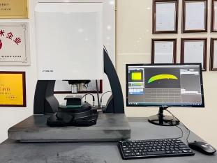
Current ultra-precision machining (such as semiconductor wafers, optical lenses, precision moulds and MEMS devices) now requires surface topography at the sub-nanometre level, yet traditional inspection methods each have their limitations: contact probes are prone to scratching the surface and can only capture line profiles; whilst atomic force microscopy (AFM) offers extremely high precision, its limited measurement range and slow speed make it difficult to meet the efficiency requirements for mass-production spot checks; Confocal microscopes typically have a vertical resolution in the hundreds of nanometres, making them unable to accurately characterise ultra-smooth surfaces.
White-light interferometric 3D profilometers, however, strike the perfect balance between accuracy, speed and applicability—utilising the principle of low-coherence light interference, they acquire full-field-of-view 3D data through vertical scanning. The measurement process is entirely non-contact, and a single measurement takes only a few seconds to cover a millimetre-scale field of view whilst maintaining a vertical resolution of 0.1 nm, providing an ideal solution for quality control that combines precision with high throughput.
In practical applications, this instrument demonstrates exceptional adaptability to a wide range of materials: it can reliably acquire interference signals from polished metal surfaces with reflectance levels exceeding 90 per cent, right through to black rubber or carbon fibre materials with reflectance levels of less than 1 per cent. The standard vertical scanning range of the instrument extends to several millimetres, and when combined with objectives offering a wide range of magnifications (2.5x–100x), it allows for seamless switching between macro-contour and micro-roughness analysis modes.

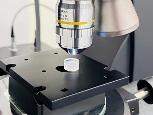
Taking the inspection of moulds for optical lens compression moulding as an example, the equipment can consistently measure surface roughness (Sa) values below 0.5 nm, whilst clearly displaying the depth and spacing of machining marks, thereby providing quantitative evidence for the optimisation of process parameters; in the inspection of semiconductor silicon wafers, the equipment can complete a flatness assessment across the entire field of view in a single pass, with RMS repeatability better than 0.03 nm, and data reliability that meets the stringent standards of production lines. Furthermore, the accompanying software supports automatic image stitching, batch measurement and real-time data analysis, significantly reducing errors associated with manual assessment. Consequently, white-light interferometric 3D profilometers are replacing traditional inspection equipment and becoming an indispensable quality control tool in ultra-precision manufacturing production lines.
Product recommendation
TECHNICAL SOLUTION
MORE+You may also be interested in the following information
FREE CONSULTING SERVICE
Let’s help you to find the right solution for your project!
 ASK POMEAS
  PRICE INQUIRY
  REQUEST DEMO/TEST
  FREE TRIAL UNIT
  ACCURATE SELECTION
- APPICATION CASE
- RESOURCE CENTER
- DOWNLOAD CENTER
SOLUTIONS SUPPORT
- ZOOM LENS SELECTION TOOL
- TELECENTRIC LENS SELECTION TOOL
- FA LENS SELECTION TOOL
- ZOOM RATIO TABLE
- CERTIFIED MODEL
SELECTION TOOL
- WHY POMEAS
- FAQ
- PRIVACY POLICY
- TERMS OF USE
- DELIVERY & RETURN POLICY
CUSTOMER CARE
 ADDRESS
Add.:No.68, Yongwei Road, Baizhoubian, Dongcheng District, Dongguan, China,523000
CONTACT
 Tel:+ 86-0769-2266 0867
 Fax:+ 86-0769-2266 0867
 E-mail:marketing@pomeas.com

Wechat QR code

Software Copyright :2021SR0176001 抄袭必究, 技术支持:誉新源科技