


How can microscopic systems be used to improve accuracy in wafer inspection?
In the semiconductor manufacturing process, wafer inspection is a critical stage for ensuring product yield. As manufacturing processes continue to advance into the nanometre range, the circuits and structures on the wafer surface are becoming increasingly intricate; cracks, particle contamination and etching deviations at the micrometre or even sub-micrometre level can all lead to chip failure. Traditional inspection methods are no longer able to meet the demands of mass production for both high precision and high efficiency. Microscopy systems equipped with high-quality ZOOM LENSes are emerging as the key solution for overcoming accuracy bottlenecks in the wafer inspection process.

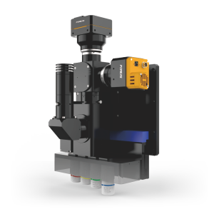
Accuracy Challenges In Wafer Inspection: Micro- and Nano-scale Defects Are Easily Overlooked

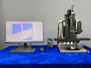
Wafer manufacturing involves dozens of processes, including lithography, etching and deposition, during which various microscopic defects are highly likely to be introduced. Such defects are extremely small and vary greatly in form; manual visual inspection is inefficient and prone to missed defects or misjudgements due to operator fatigue or other factors. Conventional optical inspection equipment is limited by its resolution and focusing capabilities; when faced with minute surface irregularities and high-density structures on the wafer, it struggles to produce stable, clear images and is unable to accurately identify and quantify defects, which directly limits inspection accuracy and the efficiency of process optimisation.
High-resolution Zoom Imaging: Precisely Capturing Defect Details

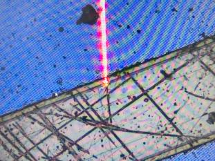
The inspection accuracy of a microscopy system is founded, first and foremost, on high-quality optical imaging. Microscopy equipment fitted with a continuously variable ZOOM LENS enables stepless magnification adjustment across a wide range, allowing for a seamless transition from a global overview of the wafer to the magnified observation of local defects without the need to change lenses. The high-resolution optical design clearly reproduces the micro- and nano-structures on the wafer surface, enabling the precise identification of various defects such as hidden cracks, micro-particles and uneven etching. It accurately depicts the morphology, size and distribution characteristics of defects, providing reliable visual evidence for subsequent defect analysis and reducing the rate of missed detection of minute defects at source.
Laser Auto-Focus, Ensuring Consistency in Batch Inspection

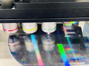
Long-term stability in inspection accuracy depends on an efficient and reliable focusing mechanism. The laser autofocus microscopy system utilises the principle of active laser ranging for focusing, overcoming the limitations of traditional manual and passive focusing methods, and is capable of rapidly locking onto the optimal focal plane within milliseconds. Addressing issues commonly encountered in mass production scenarios—such as wafer warpage, thickness tolerances and workstation height deviations—laser autofocus compensates for height differences in real time, ensuring that every inspection area remains in sharp focus and preventing false defect detections caused by focusing errors. The entire process requires no manual intervention, significantly enhancing the repeatability and consistency of batch inspection, and is well-suited to the fast-paced, in-line inspection requirements of production lines.
Practical Application: Driving Yield Improvements through Enhanced Accuracy
In mass-production wafer inspection scenarios, this microscopy system can be integrated into multiple process steps to perform either in-line spot checks or 100 per cent inspection. The high-definition images captured by the system can be used in conjunction with vision algorithms to automatically classify defects and determine their coordinates; the inspection data can be integrated with the production management system, helping process engineers to quickly identify problematic process steps and adjust process parameters. Compared with traditional inspection solutions, this microscopy system—equipped with a ZOOM LENS and laser autofocus—significantly improves the detection rate of minute defects whilst reducing the inspection time per wafer. By enhancing inspection accuracy, it effectively lowers the wafer scrap rate and contributes to a steady improvement in production line yield.
Product recommendation
TECHNICAL SOLUTION
MORE+You may also be interested in the following information
FREE CONSULTING SERVICE
Let’s help you to find the right solution for your project!
 ASK POMEAS
  PRICE INQUIRY
  REQUEST DEMO/TEST
  FREE TRIAL UNIT
  ACCURATE SELECTION
- APPICATION CASE
- RESOURCE CENTER
- DOWNLOAD CENTER
SOLUTIONS SUPPORT
- ZOOM LENS SELECTION TOOL
- TELECENTRIC LENS SELECTION TOOL
- FA LENS SELECTION TOOL
- ZOOM RATIO TABLE
- CERTIFIED MODEL
SELECTION TOOL
- WHY POMEAS
- FAQ
- PRIVACY POLICY
- TERMS OF USE
- DELIVERY & RETURN POLICY
CUSTOMER CARE
 ADDRESS
Add.:No.68, Yongwei Road, Baizhoubian, Dongcheng District, Dongguan, China,523000
CONTACT
 Tel:+ 86-0769-2266 0867
 Fax:+ 86-0769-2266 0867
 E-mail:marketing@pomeas.com

Wechat QR code

Software Copyright :2021SR0176001 抄袭必究, 技术支持:誉新源科技