


Spectral Confocal Displacement Sensor: Solder Paste Thickness Measurement on PCBs
I. Core Principles of Solder Paste Thickness Measurement on PCBs Using Spectral Confocal Displacement Sensors

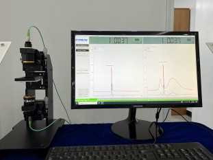
Spectral confocal displacement sensors achieve high-precision measurements based on the principles of white light dispersion and confocal imaging: After wide-spectrum white light is dispersed by a special lens assembly, light of different wavelengths forms a continuous series of monochromatic focal points along the optical axis. Only the light of a specific wavelength—whose focal point falls precisely on the surface of the solder paste—is reflected back to the spectrometer. By decoding this wavelength, the system can precisely calculate the distance to the solder paste surface. Combined with the differential measurement method, which simultaneously collects reference surface data from the bare PCB substrate, the system performs real-time differential calculations to directly determine the net thickness of the solder paste, with a measurement resolution reaching the submicron level.

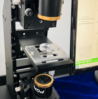
The measurement method is not affected by fluctuations in light intensity or variations in the reflectivity of PCB pads. Even in the slightly vibrating environment of an SMT production line, the differential calculation based on data collected simultaneously by the dual probes can offset most of the displacement errors caused by in-phase vibrations, ensuring the stability of the inspection data.
II. Key Criteria for Solder Paste Thickness Inspection

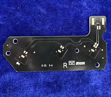
- Thickness Tolerance: On standard SMT production lines, solder paste thickness tolerance must be controlled within ±15 μm. When using SPI for 100% inspection, the accuracy requirement increases to ±10 μm; any deviation outside this range is classified as a solder deficiency or excess defect.
- Printing Quality: Solder paste must be centered over the pads, free of abnormalities such as misalignment, solder bridges, unevenness, or solder spikes. Pad coverage must be ≥90% to prevent cold solder joints or bridging during subsequent soldering.
- Uniformity Requirements: The difference in solder paste thickness between different pads on the same PCB must be controlled within 5 μm to ensure consistent soldering for all components.
III. Comprehensive Defect Inspection Solution for Post-SMT Assembly
Spectral confocal displacement sensors can perform simultaneous, multidimensional precision inspection after surface-mount assembly, covering all defect types specified by the user:
- Component Misalignment Detection: By using sensors to capture the 3D coordinates of the component surface relative to the pad reference plane, the system calculates the component’s X/Y-axis offset. A misalignment exceeding 25% of the component’s width for surface-mount components, or 15% of the pin width for precision packages such as QFPs, is classified as a misalignment defect.
- Reverse Mounting/Polarity Detection: Utilizing high-precision 3D contour scanning, this process identifies the spatial positions of component lead layouts and polarity markings to quickly determine whether a component has been mounted in the wrong orientation. It is particularly suitable for devices with specific polarity requirements, such as LEDs and electrolytic capacitors.
- Missing/Wrong Component Detection: By comparing measured height data from the placement area against a preset database of standard component heights, areas not covered by a component are identified as missing, and components with a height deviation from the standard value exceeding the threshold are identified as wrong components.
Product recommendation
TECHNICAL SOLUTION
MORE+You may also be interested in the following information
FREE CONSULTING SERVICE
Let’s help you to find the right solution for your project!

 ASK POMEAS
  PRICE INQUIRY
  REQUEST DEMO/TEST
  FREE TRIAL UNIT
  ACCURATE SELECTION
- APPICATION CASE
- RESOURCE CENTER
- DOWNLOAD CENTER
SOLUTIONS SUPPORT
- ZOOM LENS SELECTION TOOL
- TELECENTRIC LENS SELECTION TOOL
- FA LENS SELECTION TOOL
- ZOOM RATIO TABLE
- CERTIFIED MODEL
SELECTION TOOL
- WHY POMEAS
- FAQ
- PRIVACY POLICY
- TERMS OF USE
- DELIVERY & RETURN POLICY
CUSTOMER CARE
 ADDRESS
Add.:No.68, Yongwei Road, Baizhoubian, Dongcheng District, Dongguan, China,523000
CONTACT
 Tel:+ 86-0769-2266 0867
 Fax:+ 86-0769-2266 0867
 E-mail:marketing@pomeas.com

Wechat QR code

Software Copyright :2021SR0176001 抄袭必究, 技术支持:誉新源科技