


Case Study: Online Observation of Laser Chip Decapsulation Using a 14X Zoom Lens
I. Testing Background
The client is a laser equipment manufacturer that primarily integrates equipment such as laser die-opening and laser wire-stripping machines; its end customers are semiconductor chip manufacturers. During the chip die-opening process, lasers are used to remove packaging materials—such as plastic encapsulants, silicone, and underfill—layer by layer. It is necessary to monitor the die-opening depth, area contours, and die exposure in real time during processing, and to conduct surface quality inspections simultaneously after die-opening. The client aims to perform online inspection directly at the laser decapsulation station to reduce the need for offline re-inspection.
II. Testing Requirements
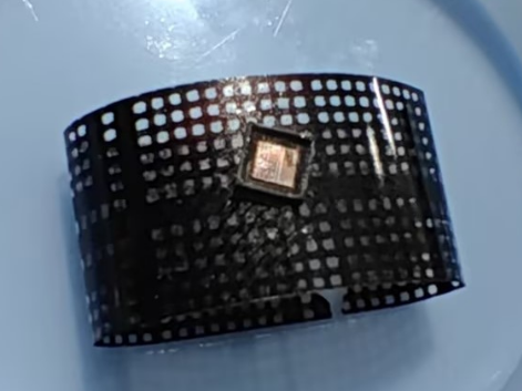
The application requires an observation system capable of real-time imaging. At low magnification, the system must quickly locate the entire chip and complete positioning; at high magnification, it must observe the edges of the laser-decapsulated chip, the removal status of the packaging material, and the surface of the bare die. Frequent lens changes or workpiece movement are not desired during the zoom process. Additionally, the system must be compatible with a 12-megapixel industrial camera and capable of storing images of the decapsulation process for verification and traceability purposes.
III. Challenges in Testing
The customer’s original solution relied on fixed-magnification microscopes or manual visual inspection, which offered only a single magnification level. At low magnification, the entire chip could not be clearly visualized for positioning, while at high magnification, the field of view was too small. This required repeated switching between magnifications for positioning, alignment, and inspection, resulting in low efficiency. Traditional microscopes have a short working distance and a bulky structure, making it difficult to position them at an angle to reach into the laser processing area. As a result, the laser-treated surface and the internal state of the cavity are hard to observe, and the quality of the decapsulation process often requires offline inspection only after the chip has been removed.
Standard lenses have a relatively short working distance and are easily contaminated by laser fumes and spatter. After decapsulation, the cavity’s surface features significant depth variations, and when the depth of field is insufficient, the image tends to be partially sharp and partially blurry. After the customer upgraded to a 12-megapixel camera, the original lens exhibited inconsistent resolution between the center and edges, insufficient MTF, and blurred, trailing images at the edges, resulting in underutilization of the pixel resolution; standard zoom lenses have poor focus consistency, requiring refocusing every time the magnification is changed, making them difficult to use directly on automated production lines.
IV. Solutions
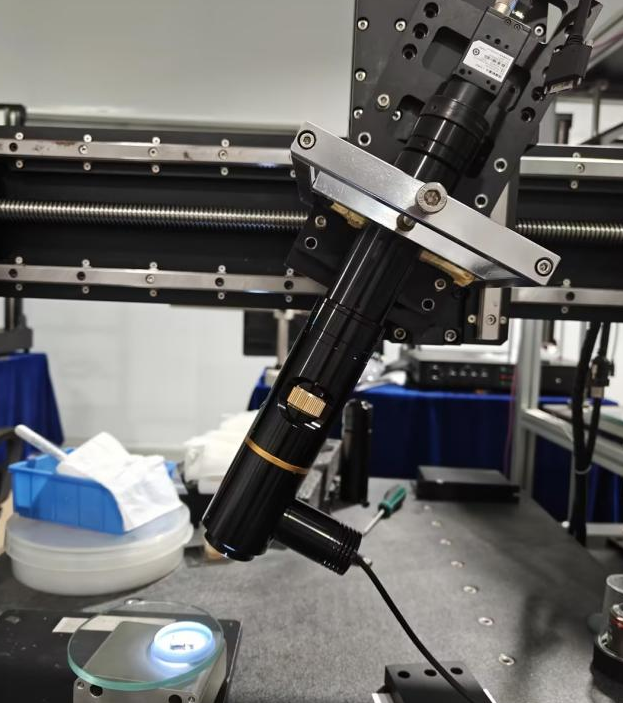
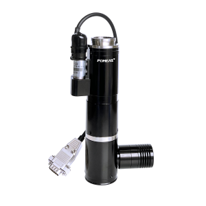
The recommended solution is a Promis 14X continuously variable industrial lens paired with a 12-megapixel industrial camera. The lens and camera assembly are mounted at an angle above the processing station of the laser die-attaching equipment, positioned to avoid the laser beam path while aligning with the die-attaching area. This configuration captures clear, wide-angle images of the die-attaching area without interfering with the laser head.
Key optical performance characteristics of the lens include: 14X continuous zoom with continuously adjustable magnification; low magnification allows for rapid chip location and positioning, while high magnification enables detailed observation of the laser decapsulation edges and the bare die surface; a single lens covers the entire “positioning—monitoring—inspection” process; High-resolution design optimized for high-pixel-count industrial cameras, with excellent full-field-of-view MTF performance. When paired with a 12-megapixel camera, it clearly captures details of chip circuits and laser ablation edges, maintaining consistent sharpness from the center to the edges; focus stability ensures the focal plane remains stable during zoom, eliminating the need for repeated refocusing and enabling programmable magnification switching when integrated with automated equipment; Long working distance and deep depth of field allow the lens to be positioned far from the processing surface, helping to reduce contamination from laser fumes and damage from spatter, while also providing space for angled installation; even at an oblique viewing angle, the height difference in the front and back of the decapsulation area remains clearly visible as a whole.
During system operation, the low-magnification end is first used to capture a panoramic view of the entire chip, quickly completing alignment and positioning; It then smoothly switches to the desired magnification. Thanks to the co-focal design, the focal plane and the center of the field of view remain essentially unchanged, allowing for zone-by-zone observation of the laser decapsulation edges, the removal status of the packaging material, and the surface of the bare die; Combined with high-resolution imaging from a 12-megapixel camera, the system monitors decapsulation depth and area contours in real time, saves the images, and outputs high-definition image data that can be used for evaluation and traceability.
V. Advantages of the Proposal
The solution features a Promis 14X continuous zoom lens paired with a 12-megapixel industrial camera, mounted at an angle on the processing station of the laser opening equipment to enable in-line monitoring that allows for “viewing while opening” and “inspection immediately after opening.”
① Low-magnification positioning and high-magnification inspection are performed with a single lens, eliminating the need to change lenses or move the workpiece, thereby shortening the inspection cycle time for individual chips;
② The entire laser de-encapsulation process is fully visible, allowing operators to instantly adjust laser power and path, reducing over-cutting, under-cutting, and chip damage, which helps improve yield;
③ The tilted mounting and long working distance design integrate the observation system with the laser processing, enabling imaging immediately upon completion of the opening process and eliminating the need for manual chip retrieval and re-inspection;
④ With 12-megapixel resolution, the images are rich in detail and can be used for process documentation, yield analysis, and customer reports, making them suitable for deployment in online observation scenarios for semiconductor processing such as laser opening and laser wire stripping.
TECHNICAL SOLUTION
MORE+You may also be interested in the following information
FREE CONSULTING SERVICE
Let’s help you to find the right solution for your project!
 ASK POMEAS
 PRICE INQUIRY
 REQUEST DEMO/TEST
 FREE TRIAL UNIT
 ACCURATE SELECTION

- APPICATION CASE
- RESOURCE CENTER
- DOWNLOAD CENTER
SOLUTIONS SUPPORT
- ZOOM LENS SELECTION TOOL
- TELECENTRIC LENS SELECTION TOOL
- FA LENS SELECTION TOOL
- ZOOM RATIO TABLE
- CERTIFIED MODEL
SELECTION TOOL
- WHY POMEAS
- FAQ
- PRIVACY POLICY
- TERMS OF USE
- DELIVERY & RETURN POLICY
CUSTOMER CARE
 ADDRESS
Add.:No.68, Yongwei Road, Baizhoubian, Dongcheng District, Dongguan, China,523000
CONTACT
 Tel:+ 86-0769-2266 0867
 Fax:+ 86-0769-2266 0867
 E-mail:marketing@pomeas.com

Wechat QR code

Software Copyright :2021SR0176001 抄袭必究, 技术支持:誉新源科技