


Case Study: Testing of Ceramic-Substrate High-Frequency and Radio-Frequency Circuit Boards
I. Background to the Testing:
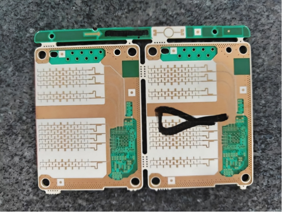
1. Test object: Ceramic-based high-frequency RF circuit boards
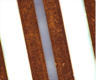
2. Requirements: A high-definition, high-precision variable-magnification vision solution is required to capture clear images of the brightness in the gold finger areas of the circuit boards, obtain clear images of the gold finger edges and the ceramic substrate, and measure line width dimensions.
3. Inspection Challenges: The gold fingers are narrower on the top layer and wider on the bottom layer, with a difference of approximately 0.005 mm between the two sides. Distinguishing the edges of the top and bottom layers requires a high magnification. Traditional ZOOM LENS vision systems fail to achieve the required magnification and suffer from poor image clarity.
II. Solutions
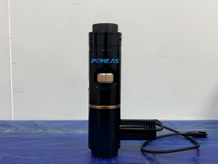
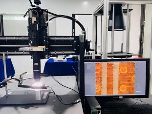
Using a 5-megapixel 2/3-inch colour camera in conjunction with the 63010+14105-K+14620 optical system, place the ceramic circuit board within the camera’s field of view, then open the measurement demo to view the positions on the circuit board that need to be measured.
III. Advantages of the Proposal

1. Optical zoom range of 1.1X to 15.2X, offering high magnification and wide coverage;
2. Ultra-low distortion design, enabling high-precision data acquisition without the need for distortion correction;
3. Full support for 2/3-inch sensor sizes, delivering high image uniformity;
4. Features absolute zero-point control technology, ensuring consistency when resetting to zero magnification;
5. Each lens is precisely calibrated to ensure optimal performance upon dispatch.
IV. Application Results

1. One machine, two functions: efficiency improved by 40%+
There is no need to change lenses; the lens in this solution can be configured with a navigation module. It first performs a wide-field, full-board scan to locate the gold fingers, followed by high-magnification inspection for precise dimensional checks and defect re-inspection. Compared to the frequent lens changes and repeated calibration required with fixed-focus lenses, the inspection time per unit has been reduced from 30 seconds to 5–8 seconds, making it suitable for in-line batch inspection and 2D rapid inspection stations.
2. Excellent compatibility with slight PCB warping
The depth-of-field design has been optimised; even with slight PCB warping or variations in gold finger plating height of ≤0.2 mm, the entire edge of the lead remains in focus, preventing edge detection failures caused by localised blurring. This makes it suitable for measuring gold fingers on FPCs and flexible circuit boards. It offers excellent installation compatibility.
Product recommendation
TECHNICAL SOLUTION
MORE+You may also be interested in the following information
FREE CONSULTING SERVICE
Let’s help you to find the right solution for your project!

 ASK POMEAS
  PRICE INQUIRY
  REQUEST DEMO/TEST
  FREE TRIAL UNIT
  ACCURATE SELECTION
- APPICATION CASE
- RESOURCE CENTER
- DOWNLOAD CENTER
SOLUTIONS SUPPORT
- ZOOM LENS SELECTION TOOL
- TELECENTRIC LENS SELECTION TOOL
- FA LENS SELECTION TOOL
- ZOOM RATIO TABLE
- CERTIFIED MODEL
SELECTION TOOL
- WHY POMEAS
- FAQ
- PRIVACY POLICY
- TERMS OF USE
- DELIVERY & RETURN POLICY
CUSTOMER CARE
 ADDRESS
Add.:No.68, Yongwei Road, Baizhoubian, Dongcheng District, Dongguan, China,523000
CONTACT
 Tel:+ 86-0769-2266 0867
 Fax:+ 86-0769-2266 0867
 E-mail:marketing@pomeas.com

Wechat QR code

Software Copyright :2021SR0176001 抄袭必究, 技术支持:誉新源科技