


Semiconductor Chip Inspection: Are Image Measurement Instruments Effective?
As the core component of the semiconductor supply chain, the dimensional accuracy of chips directly determines the yield rates of subsequent packaging, surface-mount, and assembly processes.
Chips are inherently tiny and have intricate contours. Manual measurement methods using traditional calipers and microscopes are not only inefficient but also prone to human reading errors, making it difficult to consistently meet micrometer-level dimensional control requirements. Companies urgently need a two-dimensional dimensional inspection solution that combines high precision with high-volume testing capabilities to ensure consistent quality control of key two-dimensional parameters such as chip length and width.


To address the challenges of two-dimensional dimension inspection for chips, the IMAGE 3 PRO image measurement system is used to perform inspection tasks. The system relies on high-precision industrial cameras to capture clear images of the chips. Combined with specialized vision algorithms, it automatically identifies the chip’s edge contours and calculates two-dimensional dimensional parameters such as length and width. With a measurement accuracy of up to 0.002 mm, it precisely meets chip design tolerance requirements and provides reliable data support for quality control in semiconductor production.

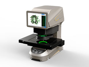
1. The device features a dual-magnification, dual-measurement mode, allowing for flexible switching between inspection settings. High-precision mode offers a 6×6 mm field of view with a repeatability of ±0.25 μm, making it ideal for verifying the fine dimensions of microchips; wide-field mode offers a 25×25 mm field of view with a repeatability of ±0.5 μm, suitable for rapid, simultaneous spot-checking of multiple chips. A single device covers both precision verification and production-line batch inspection, eliminating the need to switch between multiple instruments and reducing equipment investment costs.
2. The multi-source composite lighting configuration is key to stable chip imaging. The free combination and adjustment of various light sources—including annular light, gap light, contour backlight, and coaxial light—effectively reduce reflective interference on the chip surface, clearly outline complex contour edges, and resolve issues such as blurred imaging and difficulty in capturing edges of tiny semiconductor workpieces, thereby ensuring the stability of measurement data.
3. The system comes with the proprietary AI-Image software, which is easy to learn and user-friendly. It supports simultaneous recognition of multiple workpieces and one-click batch measurement, eliminating the need for complex programming or debugging. With a minimum display resolution of 0.1 μm, measurement data is automatically saved upon completion, facilitating quality traceability. This significantly reduces errors caused by manual operations and adapts to the high-frequency inspection pace of production lines.
4. The entire unit features an industrial-grade, stable structural design and is equipped with a 12-megapixel telecentric optical system that effectively suppresses imaging distortion and ensures dimensional measurement consistency within the field of view. The worktable supports a load capacity of 5 kg, boasts high structural rigidity, and maintains excellent stability during prolonged continuous inspection, making it suitable for routine quality inspection in semiconductor manufacturing facilities.
5. In two-dimensional chip dimension inspection scenarios, the image measuring instrument employs a non-contact optical inspection method that balances micron-level precision with batch inspection efficiency. It effectively addresses industry pain points such as the difficulty of inspecting tiny semiconductor components and unstable data, thereby promoting the standardization and automation of quality control in chip production processes.

TECHNICAL SOLUTION
MORE+You may also be interested in the following information
FREE CONSULTING SERVICE
Let’s help you to find the right solution for your project!
 ASK POMEAS
 PRICE INQUIRY
 REQUEST DEMO/TEST
 FREE TRIAL UNIT
 ACCURATE SELECTION

- APPICATION CASE
- RESOURCE CENTER
- DOWNLOAD CENTER
SOLUTIONS SUPPORT
- ZOOM LENS SELECTION TOOL
- TELECENTRIC LENS SELECTION TOOL
- FA LENS SELECTION TOOL
- ZOOM RATIO TABLE
- CERTIFIED MODEL
SELECTION TOOL
- WHY POMEAS
- FAQ
- PRIVACY POLICY
- TERMS OF USE
- DELIVERY & RETURN POLICY
CUSTOMER CARE
 ADDRESS
Add.:No.68, Yongwei Road, Baizhoubian, Dongcheng District, Dongguan, China,523000
CONTACT
 Tel:+ 86-0769-2266 0867
 Fax:+ 86-0769-2266 0867
 E-mail:marketing@pomeas.com

Wechat QR code

Software Copyright :2021SR0176001 抄袭必究, 技术支持:誉新源科技