


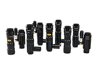
The semiconductor industry has the most demanding requirements for optical systems of any field I have encountered. Whether it’s defect re-inspection in front-end wafer processing or wire bonding measurement in back-end packaging, ZOOM LENSes address the dual challenges of inspection efficiency and precision.

Let’s address a very practical pain point: there are simply too many different package types. Today, the production line is running 0.2mm micro-components, and tomorrow it switches to a 50mm FCBGA large substrate. If fixed-magnification lenses are used, changing setups requires swapping lenses, recalibrating, and adjusting the light source—it’s common for the production line to be shut down for one or two hours. POMEAS’s motorized zoom solution, combined with autofocus, allows for one-click magnification switching via software, reducing changeover time to just a few minutes—which significantly boosts equipment utilization rates.
Another major challenge is depth of field: in semiconductor packaging, chip stacking, lead height, and solder ball coplanarity all require 3D measurement. At high magnifications, the depth of field is extremely shallow, and even slight warping can result in blurry images. This is where the advantage of a ZOOM LENS becomes apparent—I can flexibly select a compromise magnification while maintaining resolution, ensuring the depth of field covers the entire inspection area. When combined with coaxial illumination, it effectively eliminates glare on highly reflective surfaces like wafers, revealing even the finest scratches and foreign particles.
Illumination: Both wafers and lead frames are highly reflective surfaces; standard illumination easily causes glare, obscuring fine scratches and foreign particles. Engineers typically opt for coaxial incident illumination, where light strikes the surface of the object under inspection perpendicularly, and the reflected light returns along the same path into the lens, effectively suppressing surface reflections. POMEAS’s zoom modules offer comprehensive support in this regard, allowing for flexible combinations of coaxial and annular light interfaces to accommodate the inspection requirements of different materials.
Product recommendation
TECHNICAL SOLUTION
MORE+You may also be interested in the following information
FREE CONSULTING SERVICE
Let’s help you to find the right solution for your project!

 ASK POMEAS
  PRICE INQUIRY
  REQUEST DEMO/TEST
  FREE TRIAL UNIT
  ACCURATE SELECTION
 - APPICATION CASE
- RESOURCE CENTER
- DOWNLOAD CENTER
SOLUTIONS SUPPORT
- ZOOM LENS SELECTION TOOL
- TELECENTRIC LENS SELECTION TOOL
- FA LENS SELECTION TOOL
- ZOOM RATIO TABLE
- CERTIFIED MODEL
SELECTION TOOL
- WHY POMEAS
- FAQ
- PRIVACY POLICY
- TERMS OF USE
- DELIVERY & RETURN POLICY
CUSTOMER CARE
 ADDRESS
Add.:No.68, Yongwei Road, Baizhoubian, Dongcheng District, Dongguan, China,523000
CONTACT
 Tel:+ 86-0769-2266 0867
 Fax:+ 86-0769-2266 0867
 E-mail:marketing@pomeas.com

Wechat QR code
Software Copyright :2021SR0176001 抄袭必究, 技术支持:誉新源科技