


Applications of 14K ZOOM LENSES: Inspection of ceramic-based high-frequency PCBs
With the rapid development of the high-frequency communications and precision RF electronics industries, ceramic-based high-frequency PCBs have become the core substrate for high-end precision electronic equipment, thanks to their key advantages such as excellent thermal conductivity, stable high-frequency signal transmission, high-temperature resistance and low loss. Such circuit boards feature intricate structures and extremely tight dimensional tolerances; in particular, the forming precision of the gold finger areas directly affects the board’s electrical conductivity and product stability. Consequently, visual inspection during the production process is subject to extremely high industry standards regarding image clarity, magnification accuracy, dimensional measurement precision and inspection efficiency.

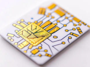
I. Customer Testing Requirements
The focus of this inspection is on conducting comprehensive, high-precision testing of the gold finger areas on ceramic-based high-frequency PCBs. Companies must use specialist vision equipment to capture clear, full-area images of the PCB gold fingers, accurately depicting the edge contours of the gold fingers and the details of the ceramic substrate, whilst simultaneously performing high-precision dimensional measurements of the gold finger line widths. This ensures strict control over product manufacturing accuracy and prevents defective products from entering the next stage of production.
II. Challenges in Industry Testing

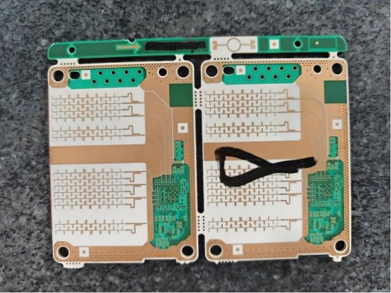
The ceramic-based high-frequency PCB gold fingers to be inspected in this instance feature a special dual-layer structure, with the upper layer narrower than the lower one. The dimensional difference between the two sides is merely 0.005 mm; such micrometre-level variations place extremely high demands on imaging magnification and image clarity, necessitating the use of high-magnification optical equipment to accurately distinguish the edge boundaries of the dual-layer gold fingers.
The ZOOM LENSes used in traditional vision inspection have an upper limit on optical magnification that fails to meet the high-precision resolution requirements of this scenario. Under high-magnification observation, the image is prone to issues such as edge blurring, loss of detail and insufficient contrast, making it difficult to accurately identify the boundaries of the dual-layer gold fingers. Furthermore, traditional fixed-focus lenses offer limited adaptability; the inspection process requires frequent lens changes and repeated calibration, which not only compromises inspection accuracy but also significantly increases processing time, making it difficult to meet the production demands of industrial-scale batch inspection.
III. POMEAS 14K ZOOM LENS Solution

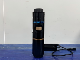
Addressing the challenges of precision inspection for ceramic-based high-frequency PCBs, the POMEAS 14K ZOOM LENS, with its outstanding optical performance and proprietary technological advantages, provides an efficient, accurate and stable integrated vision inspection solution, effectively overcoming the industry’s inspection shortcomings.
The lens features an exceptionally wide optical zoom range, allowing for seamless switching between field-of-view magnifications to meet the dual requirements of wide-area scanning and micrometre-level precision inspection. Furthermore, the system is equipped with absolute zero-point control technology, ensuring that the magnification remains highly consistent every time the lens resets to zero. This completely eliminates issues such as magnification drift and calibration errors, thereby guaranteeing the stability of each image and the accuracy of inspection data at the source.

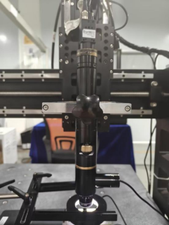
During the actual inspection process, the lens enables efficient inspection in dual modes: using the low-magnification, wide-field-of-view mode of the 14X ZOOM LENS, it rapidly performs a comprehensive scan of the entire gold-finger area on the PCB, precisely locating all inspection areas and completing an initial screening of the entire board; it then seamlessly switches to high-magnification mode to carry out precise measurements of the gold-finger edges and line widths, whilst simultaneously conducting a detailed re-inspection for surface defects, thereby completing the entire inspection process in a single step.
IV. Advantages and Benefits of the Scheme’s Implementation

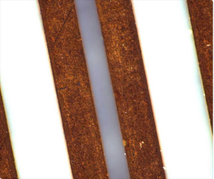
Compared to the cumbersome operation of traditional fixed-focus lenses, the POMEAS 14K ZOOM LENS eliminates the need for frequent equipment changes and repeated calibration, thereby greatly simplifying the inspection process and significantly improving inspection efficiency.
The 14X ZOOM LENS offers exceptional versatility and can be widely applied in various scenarios, including in-line batch inspection on production lines and precision workstations for 2D flash inspection. Combining the three core advantages of high precision, high stability and high efficiency, it effectively assists enterprises in achieving automated, standardised and refined production for PCB quality inspection, comprehensively improving product yield rates and overall production line capacity, whilst providing reliable vision equipment support for quality upgrades in high-end precision electronics manufacturing.
Product recommendation
TECHNICAL SOLUTION
MORE+You may also be interested in the following information
FREE CONSULTING SERVICE
Let’s help you to find the right solution for your project!

 ASK POMEAS
  PRICE INQUIRY
  REQUEST DEMO/TEST
  FREE TRIAL UNIT
  ACCURATE SELECTION
- APPICATION CASE
- RESOURCE CENTER
- DOWNLOAD CENTER
SOLUTIONS SUPPORT
- ZOOM LENS SELECTION TOOL
- TELECENTRIC LENS SELECTION TOOL
- FA LENS SELECTION TOOL
- ZOOM RATIO TABLE
- CERTIFIED MODEL
SELECTION TOOL
- WHY POMEAS
- FAQ
- PRIVACY POLICY
- TERMS OF USE
- DELIVERY & RETURN POLICY
CUSTOMER CARE
 ADDRESS
Add.:No.68, Yongwei Road, Baizhoubian, Dongcheng District, Dongguan, China,523000
CONTACT
 Tel:+ 86-0769-2266 0867
 Fax:+ 86-0769-2266 0867
 E-mail:marketing@pomeas.com

Wechat QR code

Software Copyright :2021SR0176001 抄袭必究, 技术支持:誉新源科技