


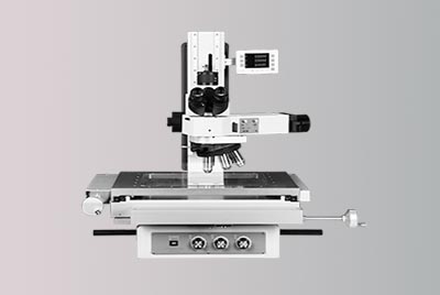
What is a tool microscope?
Tool Microscope is a mechanical optical instrument based on optical (microscopic) aiming and coordinate (worktable) measurement. It can be used to measure various lengths and angles. It is especially suitable for measuring various complex tools and parts, such as thread, cam profile, cutting tool and hole spacing, etc. It has a wide range of applications.
Tool microscopy is mainly divided into four types: small tool microscopy, large tool microscopy, universal tool microscopy and heavy universal tool microscopy. They all have the basic characteristics of tool microscopy. In addition to the differences in measuring range and grading value, other factors such as the load-carrying capacity of the worktable, the types and quantities of accessories and the accuracy of the instrument are different.
Tool Microscope Applications and Characteristics:
It is widely used in electronic components, precision die, precision tool, spring, plastic, rubber, oil seal valve, camera parts, automobile parts, PCB processing and other fields. Two-dimensional measurement is the main method, and three-dimensional auxiliary measurement can also be done. It can also be compared with standard eyepiece.
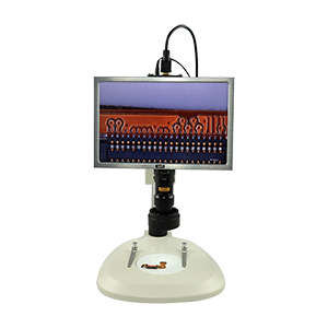
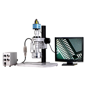
Measure the dimension of workpiece such as thread pitch, outer diameter, tooth angle, ruler and cutting tool, or magnify the outline of workpiece by microscopy, inspect the surface condition of workpiece, measure the angle and length, etc. In addition, it can also be used as an observation microscope to check the surface roughness of the workpiece by relative measurement and other non-contact measurement for the purpose of various precision processing industries.
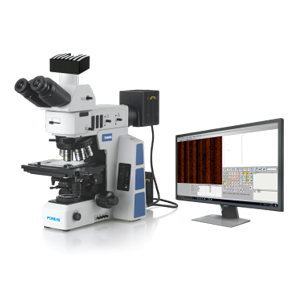
PMS-TM200 combines the high power observation ability of metallographic microscope with X, Y and Z axis surface dimension measurement function of image measuring instrument. It has many observation functions such as light and dark field, differential interference, polarization and so on. It can be widely used in semiconductor, PCB, LCD, mobile phone industry chain, optical communication, basic electronics, die hardware, medical equipment, automobile industry, measurement industry and other fields.
Product recommendation
TECHNICAL SOLUTION
MORE+You may also be interested in the following information


FREE CONSULTING SERVICE
Let’s help you to find the right solution for your project!

 ASK POMEAS
  PRICE INQUIRY
  REQUEST DEMO/TEST
  FREE TRIAL UNIT
  ACCURATE SELECTION
 - APPICATION CASE
- RESOURCE CENTER
- DOWNLOAD CENTER
SOLUTIONS SUPPORT
- ZOOM LENS SELECTION TOOL
- TELECENTRIC LENS SELECTION TOOL
- FA LENS SELECTION TOOL
- ZOOM RATIO TABLE
- CERTIFIED MODEL
SELECTION TOOL
- WHY POMEAS
- FAQ
- PRIVACY POLICY
- TERMS OF USE
- DELIVERY & RETURN POLICY
CUSTOMER CARE
 ADDRESS
Add.:No.68, Yongwei Road, Baizhoubian, Dongcheng District, Dongguan, China,523000
CONTACT
 Tel:+ 86-0769-2266 0867
 Fax:+ 86-0769-2266 0867
 E-mail:marketing@pomeas.com

Wechat QR code
Software Copyright :2021SR0176001 抄袭必究, 技术支持:誉新源科技