


Semiconductor wafer size measurement for precision visual inspection
Semiconductor silicon wafer is the core material for making chips. It runs through the whole process of chip making. The quality of the silicon wafer affects the performance of the chip, so the relative dimensional accuracy of its product features is very high.
Detection scheme:
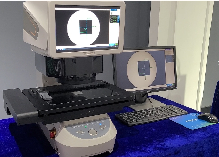
The IMAGE3 image size measuring instrument is equipped with dual 20-megapixel industrial cameras and high-magnification telecentric optical lenses, which can measure the length, width, distance, verticality and other dimensions of silicon wafers with high precision and high efficiency.
Detection process:
Place the product on the stage, load the prepared measurement program, press the start button, the program will run automatically, accurately position the product, automatically adjust the focus, and automatically identify the measurement location of the product. result. After the measurement, output data such as length, width, distance, and verticality according to customer requirements, and automatically determine whether the data meets the requirements, which is convenient for quality inspectors to quickly check whether they are qualified.
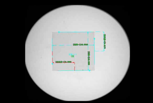
Detecting renderings:
Program advantages:
1. Only press one button to measure after placing, 100 parts can be measured in 1 second, which saves a lot of time, and can be matched with customer IO signals to achieve automatic measurement;
2. With the independent and powerful AI edge computing algorithm, it is easy to achieve precise edge finding on the surface, and the boundary noise filters the invalid area;
3. With automatic positioning, automatic focusing, and automatic measurement functions, anyone can obtain accurate and consistent results when measuring.
Pomeas image size measuring instrument has fast and accurate measurement capabilities to meet the manufacturing requirements of semiconductor precision parts. It is also widely used in mobile phones, hardware, plastic parts, watches, glass and other industries.
TECHNICAL SOLUTION
MORE+You may also be interested in the following information
Laser Profile Sensor

FREE CONSULTING SERVICE
Let’s help you to find the right solution for your project!

 ASK POMEAS
  PRICE INQUIRY
  REQUEST DEMO/TEST
  FREE TRIAL UNIT
  ACCURATE SELECTION
 - APPICATION CASE
- RESOURCE CENTER
- DOWNLOAD CENTER
SOLUTIONS SUPPORT
- ZOOM LENS SELECTION TOOL
- TELECENTRIC LENS SELECTION TOOL
- FA LENS SELECTION TOOL
- ZOOM RATIO TABLE
- CERTIFIED MODEL
SELECTION TOOL
- WHY POMEAS
- FAQ
- PRIVACY POLICY
- TERMS OF USE
- DELIVERY & RETURN POLICY
CUSTOMER CARE
 ADDRESS
Add.:No.68, Yongwei Road, Baizhoubian, Dongcheng District, Dongguan, China,523000
CONTACT
 Tel:+ 86-0769-2266 0867
 Fax:+ 86-0769-2266 0867
 E-mail:marketing@pomeas.com

Wechat QR code
Software Copyright :2021SR0176001 抄袭必究, 技术支持:誉新源科技